Summary of SCRATCH-BUILT INDUSTRIAL CAMERA’S MODULAR DESIGN REALLY STACKS UP
Guarav Singh engineered a high-quality industrial digital camera from scratch, emphasizing modularity to allow sensor swaps as technology evolves. The design features a three-PCB stack with a central FPGA board flanked by sensor and USB 3.0 boards, all housed in a custom 3D-printed case with an aluminum C-mount ring. The project provides detailed insights into FPGA data processing and practical implementation of MIPI and CSI specifications.
Parts used in the Scratch-Built Industrial Camera:
- Lattice FPGA chip
- Two 16-MB RAMs
- FPGA config flash
- Sensor board
- USB 3.0 board
- Six-layer PCBs (three total)
- 3D-printed case
- Integrated aluminum C-mount ring
The news here isn’t so much that [Guarav Singh] built this high-quality industrial digital camera from scratch, but it’s in the way it was accomplished. That plus the amount of information that’s packed into the write-up, of course. And the excellent photography.
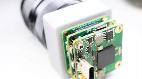
Modularity was one of [Guarav]’s design goals, with the intention of being able to swap out the sensor as the technology changes. To that end, [Guarav] came up with a stack of three PCBs. The middle board of the stack contains a Lattice FPGA chip along with two 16-MB RAMs and the FPGA config flash. The sensor board lies on one side of the FBGA board, while the USB 3.0 board is on the other. Each six-layer board is a masterpiece of high-density design, and the engineering that went into interfacing them and getting everything squeezed into a 3D-printed case with an integrated aluminum C-mount ring is pretty impressive.
[Guarav]’s write-up goes into a great deal of detail on processing the sensor data on the FPGA. Also, there’s quite a bit of practical information on implementing MIPI (Mobile Industry Processor Interface) and the CSI (Camera Serial Interface) specification. We’ve delved into this world before, but this project is a great hands-on explanation that might really help move your MIPI project along.
Source: SCRATCH-BUILT INDUSTRIAL CAMERA’S MODULAR DESIGN REALLY STACKS UP
- What was one of Guarav's main design goals?
Modularity to swap out the sensor as technology changes. - How many PCBs are stacked in the camera design?
The design uses a stack of three PCBs. - What components are located on the middle board?
The middle board contains a Lattice FPGA chip, two 16-MB RAMs, and FPGA config flash. - Where is the sensor board positioned relative to the FPGA board?
The sensor board lies on one side of the FBGA board. - What material is used for the integrated mount ring?
An integrated aluminum C-mount ring is used. - Does the write-up cover MIPI implementation details?
Yes, it includes practical information on implementing MIPI and CSI specifications. - What interface specification is mentioned alongside MIPI?
The Camera Serial Interface (CSI) specification is discussed. - Is the camera built from off-the-shelf parts or from scratch?
The article states the camera was built from scratch.