Summary of DIY Arduino UNO
This article details the process of building a custom Arduino S3v3 board compatible with UNO standards using JLC PCB. It covers schematic components like the Atmega microcontroller, voltage regulators, and various connectors (DE-9, DC jack). The guide includes step-by-step instructions for ordering PCBs via JLCPCB, uploading Gerber files, and configuring payment and shipping. Additionally, it provides critical mounting tips for component orientation and software advice for bootloading different Atmega chips to ensure successful project completion.
Parts used in the DIY Arduino S3v3:
- DE-9 serial connector
- 2.1 mm power jack
- 2x3 pin header (ICSP)
- 3 pins jumper (JP0)
- 2 pins jumper (JP4)
- Tactile button (S1)
- POWER LED
- RX LED
- TX LED
- L LED
- 6 pin header (Power Pinout)
- 8 pin header x2 (Digital In/Out Pinout)
- 6 analog inputs (Analog In Pinout)
- Atmega IC (Atmega8 or Atmega168)
- Voltage Regulator (7805)
- Bipolar electrolytic capacitor
- Diodes and Transistors
- IC socket
DIY your own Arduino UNO with the JLC PCB
Description
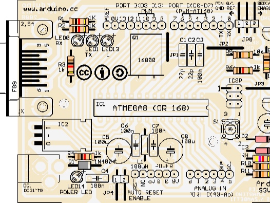
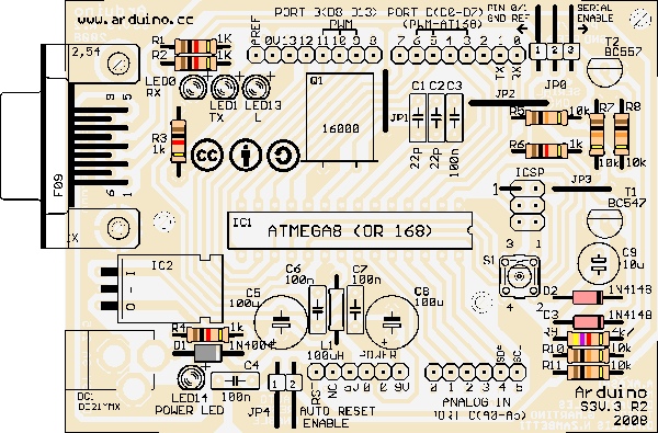
Schematic of ARDUINO S3v3
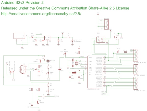
Details of ARDUINO S3v3
X1: DE-9 serial connector
Used to connect a computer (or other devices) using RS-232 standard. Needs a serial cable, with at least 4 pins connected: 2, 3, 4, and 5. Works only when JP0 is set to 2-3 position.
DC1: 2.1 mm. power jack
Used to connect the external power source. Centre positive. Voltage Regulator Works with regulated +7 to +20 volts DC (9v. to 12v. is recommended). It is possible to alternatively connect external power using 9v. pin or 5v. pin. (see POWER PINOUT)
ICSP: 2×3 pin header
Used to program Atmega with the bootloader. The number 1 on both sides of the board indicates the cable pin1 position. Used to upload sketches on Atmega ICs without bootloader (available only in Arduino IDE versions 0011 and 0012).
JP0 3 pins jumper
When in position 2-3, this jumper enables serial connection (through X1 connector) to/from computer/devices. Use this as the default position. When in position 1-2, it disables serial communication and enables external pull-down resistors on pin0 (RX) and pin1 (TX). Use this only to prevent noise on RX (that seems incoming data to Atmega), which sometimes makes sketch not starting. When removing this jumper, serial communication is disabled, and pin0 and pin1 work as normal (floating) digital pins. Useful when more digital pins are needed, but only when serial communication is not necessary. An external pull-down/pull-up resistor is required.
JP4 2 pins jumper
When in position 1-2, this jumper enables an auto-reset feature, useful when uploading a sketch to Arduino, resetting Atmega automatically. It makes unnecessary to press the reset button (S1) when uploading sketches. Be sure that computer COM Port speed is set to 19200bps otherwise auto-reset will not work properly. If removed, disables the auto-reset feature. Very useful to prevent undesired Atmega reset when using sketches that need serial communication. Auto-reset works with DTR pulse on serial pin4. Sometimes Arduino senses a DTR pulse when connecting X1 (serial connector) and some software sends a DTR pulse when it starts or when it closes, which makes Atmega reset when not desired.
S1 Tactile button
This button resets Atmega, to restart the uploaded sketch or to prepare Arduino to receive a sketch through a serial connector (when auto-reset is not active).
LED
Indicative LEDs
POWER led
Turns on when Arduino is powered through DC1, +9v. pin or +5v. pin.
RX led
Blinks when receiving data from computer/device through a serial connection.
TX led
Blinks when sending data to computer/device through a serial connection.
L led
This led is connected to digital pin13 with a current limiter resistor (that doesn’t affect pin13). Useful to test sketches. It is normal to blink when bootloading too.
POWER PINOUT
6 pin header
RST pin
Makes Atmega reset when connected to GND. Useful for Shield Boards, or to connect external reset.
NC pin
This pin is not connected in Arduino S3v3. Arduino Diecimila has a 3.3 volts pin in the same position.
+9v. pin
When Arduino DC1 is powered (with battery or DC adaptor), this pin is used as Vout, with the same voltage supplied on DC1 (see DC1), minus 0,7 volts. The total supplied current depends on external power source capacity When Arduino DC1 is not powered, +9v. the pin can be used as Vin, connecting it to an external regulated power source (+7 to +20 volts) and connecting 0v. pin to external power source GND. In this case, +5v. the pin can be used as Vout, supplying +5 volts.
+5v. pin
When Arduino DC1 is powered (with battery or DC adaptor), +5v. pin supplies +5 volts as a Vout pin. The total supplied current depends on Voltage Regulator (7805 supplies up to 1A). This applies only to +5v. pin: Atmega in/out pins only supplies max. 40mA on each pin. When Arduino DC1 is not powered, this pin can be used as Vin, connecting it to a regulated +5v. and connecting 0v. pin to power source GND. In this case, +9v. the pin is inactive.
0v. pin (GND)
Two 0v. pins between +5v. and +9v. / One 0v. pin beside AREF pin. When Arduino DC1 is powered, 0v. pin supplies 0 volts reference (GND) for +5v. pin and +9v. pin. When DC1 is not powered, and Arduino is powered through +5v. pin or +9v. pin, 0v. pin must be used as a GND reference, connecting it to the external power source GND.
DIGITAL IN/OUT PINOUT
8 pin header (x2) 8 digital inputs/outputs: 0 to 7, corresponding to Port D. Pin0 (RX) and pin1 (TX) can be used as communication pins. Pin3, pin5, and pin6 can be used as PWM pins (Atmega168 only). 6 digital inputs/outputs: 8 to 13, corresponding to Port B. Pin10 (SS), pin11 (MOSI), pin12 (MISO), and pin13 (SCK) can be used as SPI (Serial Peripheral Interface). Pin9, pin10, and pin11 can be used as PWM pins (Atmega8 and Atmega168).
ANALOG IN PINOUT
6 analog inputs: 0 to 5, corresponding to Port C. Pin4 (SDA) and pin5 (SCL) can be used with I2C (two-wire serial bus). The analog input pins can be used as digital pins with numbers 14 (analog input 0) to 19 (analog input 5).
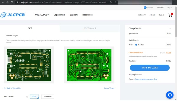
Order the PCB from JLC PCB
Step 1 –
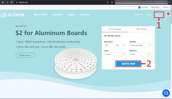
Go to the JLCPCB website using the https://jlcpcb.com/ link and create your account.
After creating an account click on QUOTE NOW.
Step 2 –
Now Upload the attached Gerber File
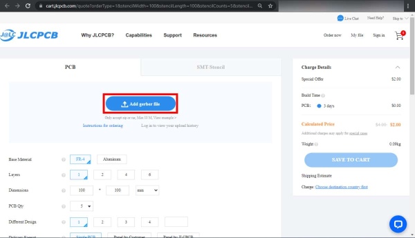
Step 2 –
Now Upload the attached Gerber File and you can check the Gerber file on Gerber viewer.
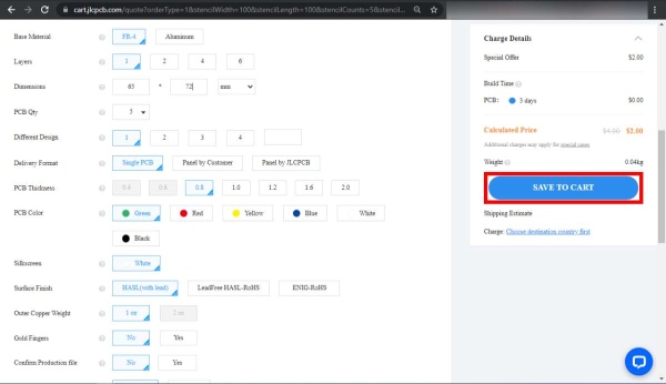
Step 3 –
Set all parameters of your PCB as shown in the below picture and, if there is no problem, just click “Save to Cart” to continue.
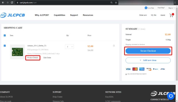
Step 4 –
Now go to your cart and check your “Product Details”, Once you have all your PCBs in the Cart click the ” Secure Checkout” button.
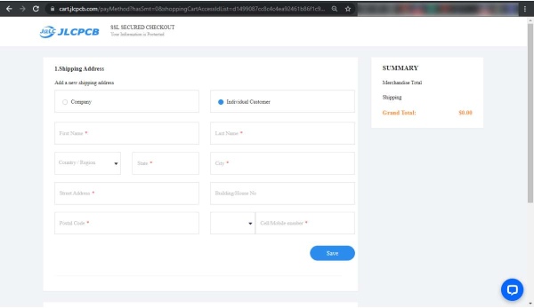
Step 5 –
On the checkout page, you add your shipping address, the country determines the shipping rate. The shipping options are below the address. DHL takes about 3-5 days to deliver (not including the 3-4 day manufacturing time), Airmail takes 15-25 days.
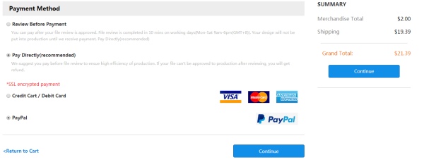
Step 6 –
They offer two kinds of payment methods.
- Review Before Payment
You can pay after your file review is approved. Your design will not be put into production until we receive payment. We’ll inform you of the results by email after reviewing them. To avoid any delays in delivery, please pay as soon as the file audit is approved. Failed audit orders will be canceled automatically. - Pay Directly(recommended)
We suggest you pay before file review to ensure high efficiency of production. If your file can’t be approved to production after reviewing, you will get a full refund.
Step 7 –
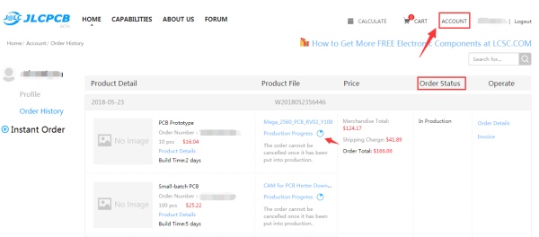
After the order payment is successful, they will arrange your production as soon as possible, during which you can through the ” ACCOUNT” menu to check your Order Status.
Component Mounting Details
Mounting Tips
Pay attention to LED’s lateral chamfer, electrolytic capacitor’s negative (-) pole mark (mounting diagram has positive (+) mark), diode’s stripe, Atmega IC’s and IC socket’s notch, and transistor’s numbers and positions. Note that similar components have the same board orientation.
Software Tips
When bootloading an Atmega8 chip with Arduino 0010, there is a command (-i800) that makes the bootloader delay 10 minutes. So, if you need to use the bootloader, use the command line instead of IDE, removing the “–i800” command and adding the “–F” command, or use Arduino 0007 IDE. To upload sketches Arduino 0010 works fine.
Features of Arduino S3v3
- full compatible with Shield Boards (Version 2 is the only Arduino Board not compatible with Shield Boards because of ICSP header wrong position, and tall components);
- AVcc LP filter to reduce noise level on ADC;
- auto-reset feature;
- auto reset enable/disable jumper, to avoid not desired resetting;
- Arduino Diecimila compatible reset pin;
- pin13 onboard led, with current limiter resistor;
- TX and RX onboard LEDs;
- power led with appropriate current limiter resistor (less than 20mA of consumption); · jumper to disable serial communication and to enable RX external pull-down resistor, to avoid “RX floating error”. This feature allows to use of digital pin0 and pin1 as a normal pin when serial communication is not needed;
- all similar components (diodes, transistors, LEDs, capacitors) has the same board orientation (to makes easier to mount with fewer mistakes);
- no wires between pads, more space between wires, larger wires, larger pads (better for etching, soldering, and drilling, with no short circuits, soldering bridges, or open wires in corrosion);
- only 3 wire bridges; · electrolytic capacitor (in serial to TTL circuit) changed to bipolar type (to avoid inverted voltage problem when the serial cable is not connected);
- All jumpers are right angle type, to allow Shield Boards use.
Source: DIY Arduino UNO
- How do I connect a computer to the Arduino S3v3?
You must use a DE-9 serial connector with at least 4 pins connected (2, 3, 4, and 5) and set JP0 to the 2-3 position. - What is the recommended voltage range for the DC power jack?
The voltage regulator works with regulated +7 to +20 volts DC, with 9v to 12v being recommended. - Can I disable the auto-reset feature on the board?
Yes, you can remove the JP4 jumper to disable the auto-reset feature. - Does the L LED affect digital pin 13 functionality?
No, the L LED is connected to digital pin 13 with a current limiter resistor that does not affect pin 13. - How do I use the +9v pin when the DC1 is not powered?
When DC1 is not powered, the +9v pin can be used as Vin by connecting it to an external regulated power source (+7 to +20 volts). - Which pins support PWM functionality on the Atmega168?
On the Atmega168, pin3, pin5, and pin6 can be used as PWM pins. - What is the best way to avoid RX floating errors?
Set the JP0 jumper to the 1-2 position to enable external pull-down resistors on pin0 and pin1. - Does this board support Shield Boards?
Yes, the Arduino S3v3 is fully compatible with Shield Boards due to its right angle jumpers and correct ICSP header position. - How can I prevent noise on the RX line if sketches do not start?
Use the JP0 jumper in the 1-2 position to enable external pull-down resistors which prevents noise on RX. - What command should be avoided when bootloading an Atmega8 chip with Arduino 0010?
You should avoid the -i800 command as it causes a 10-minute delay; instead use the -F command or switch to Arduino 0007 IDE.