Summary of Reverse engineering the silicon in the ARM1 processor
The article reverse-engineers the ARM1 processor's bit counter, a circuit that counts set bits in a 16-bit field to optimize block data transfers. It details how pass transistor logic combines NMOS and PMOS transistors into transmission gates, which form multiplexers. These multiplexers create logic gates and full adders, ultimately constructing the bit counting mechanism essential for the ARM architecture's performance.
Parts used in the ARM1 Bit Counter:
- NMOS transistors
- PMOS transistors
- Transmission gates
- Multiplexers
- Logic gates
- Full adders
- Bit counter circuit
How can you count bits in hardware? In this article, I reverse-engineer the circuit used by the ARM1 processor to count the number of set bits in a 16-bit field, showing how individual transistors form multiplexers, which are combined into adders, and finally form the bit counter. The ARM1 is the ancestor of the processor in most cell phones, so you may have a descendent of this circuit in your pocket.
ARM is now the world’s most popular instruction set but it has humble beginnings. The original ARM1 processor was designed in 1985 by a UK company called Acorn Computer for the BBC Micro home/educational computer. A few years later Apple needed a low-power, high-performance processor for its ill-fated Newton handheld system and chose ARM.[1] In 1990, Acorn Computers, Apple, and chip manufacturer VLSI Technology formed the company Advanced RISC Machines to continue ARM development. ARM became very popular for low power applications (such as phones) and now more than 50 billion ARM processors have been manufactured.
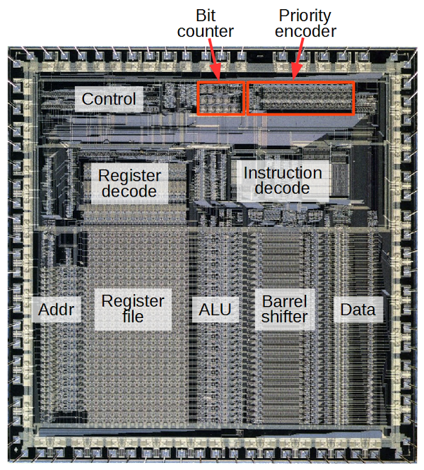
One way ARM processors increase performance is through block data transfer instructions, which efficiently copy data between on-chip registers and memory storage.[2] These instructions can transfer any subset of ARM’s 16 registers in a single instruction. The desired registers are specified by setting the corresponding bits in a 16-bit field in the instruction. To implement the block transfer instructions, the ARM requires two specialized circuits. The first circuit, the bit counter, counts the number of bits set in the register select field to determine how many registers are being transferred.[3] The second circuit, the priority encoder, scans the register select field and finds the next set bit, indicating which register to load/store next.
These two circuits are highlighted in red in the ARM1 die photo above. As you can see, the circuits take up a significant fraction of the chip (about 3%), but the chip designers felt the performance gain from block transfers was worth the increase in chip size and complexity. This article explains the bit counter, and I plan to describe the priority encoder later.
Zooming in on the bit counter reveals the circuit below. It looks like a jumble of lines, but by examining it carefully, you can get an understanding of what is going on. The remainder of the article explains how a special type of circuitry called pass transistor logic is used to build a multiplexer — a circuit that selects one of its two inputs. The multiplexers are used to form logic gates, which are then combined to form a full adder, which adds three bits. Finally, the adders are combined to create the bit counting circuit. If you’re not familiar with digital logic or the ARM processor, you might want to start with my earlier article on reverse-engineering the ARM1 for an overview.
Pass transistors and transmission gates
The bit counter is built from a type of circuitry called pass transistor logic. Unlike normal logic gates, pass transistor logic switches the inputs themselves to pass an input directly to the output. Pass transistors are used because sums (i.e. XORs) are inconvenient to generate with standard logic and can be generated more efficiently with pass transistor logic.
The ARM1 chip, like most modern chips, is built from a technology called CMOS. The C in CMOS stands for complementary because CMOS circuits are built from two complementary types of transistors. NMOS transistors switch on when the control signal on the gate is high, and can pull the output low. PMOS transistors are opposite; they switch on when the gate’s control signal is low, and can pull the output high. Combining an NMOS transistor and a PMOS transistor in parallel forms a transmission gate. If both transistors are on, the input will be passed to the output whether it is low or high. If both transistors are off, the input is blocked. Thus, the circuit acts as a switch that can either pass the input through to the output or block it.
The diagram below shows two transistors (circled) connected to form a transmission gate. The upper one is NMOS and the lower one is PMOS. On the right is the symbol for a transmission gate. Note that because the transistors are complementary, they require opposite enable signals.
Read more: Reverse engineering the silicon in the ARM1 processor
- What is the primary function of the bit counter in the ARM1 processor?
The bit counter counts the number of bits set in a 16-bit register select field to determine how many registers are being transferred during block data transfer instructions. - How does pass transistor logic differ from normal logic gates?
Unlike normal logic gates, pass transistor logic switches inputs directly to pass an input signal straight to the output rather than generating standard logic levels. - Why are transmission gates used in the ARM1 chip design?
Transmission gates combine NMOS and PMOS transistors to act as switches that can pass either a low or high input signal to the output when enabled. - What technology is the ARM1 chip built from?
The ARM1 chip is built from CMOS technology, which uses complementary types of transistors known as NMOS and PMOS. - How do NMOS transistors function within the circuit?
NMOS transistors switch on when the control signal on the gate is high and can pull the output low. - How do PMOS transistors function within the circuit?
PMOS transistors switch on when the gate's control signal is low and can pull the output high. - What is the relationship between multiplexers and the bit counter?
Multiplexers are combined to form logic gates, which are then used to create full adders that finally construct the bit counting circuit. - What percentage of the ARM1 chip does the bit counter occupy?
The bit counter and priority encoder circuits take up about 3% of the total chip size.