I came across an article on PCB layout in Electronic Design magazine. It’s a pretty good article and I am glad to see the trade magazines realize we care as much about PCB layout as the bus-caching architecture of some DSP chip. The article talks about using vias to take heat away from the die-attach-paddle (DAP) of integrated circuits:
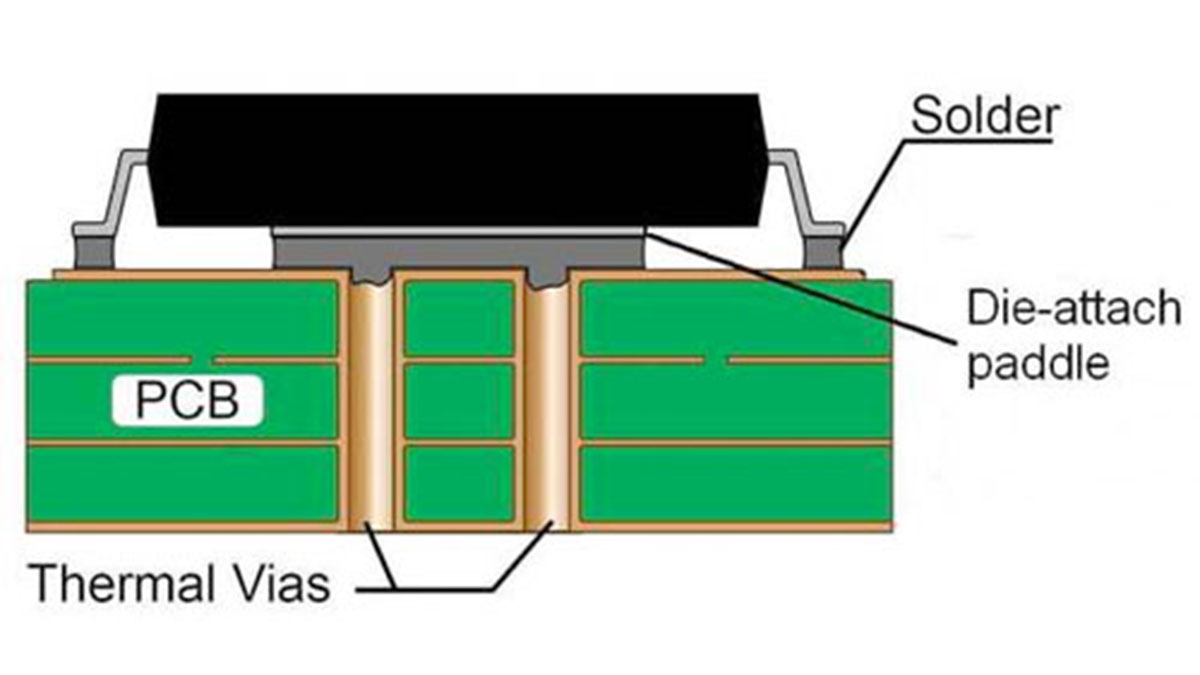
To reduce operating temperatures easily, use more layers of solid ground or power planes connected directly to heat sources with multiple vias. Establishing effective heat and high-current routes will optimize heat transfer by means of convection. The use of thermally conductive planes to spread the heat evenly dramatically lowers the temperature by maximizing the area used for heat transfer to the atmosphere.
Know there is a lot of caution you need to exercise when trying to get the heat out of a part just using a circuit board. You have to realize the guidelines in the datasheet are usually based on one part making heat, sitting on a standard board of certain dimensions. If you have a lot of hot components you can’t expect the same die temperatures for the part in question. Same goes if you have the board covered with some tight enclosure.
Texas Instruments’ WEBENCH is a neat program, especially because it has Mentor Graphic’s FloTherm built in to help you see the hot spots in switching regulators. This is what taught me that a modern buck regulator will have more heat coming out of the catch diode than the pass FET. It made perfect sense once I saw the heat diagram. After all, a diode has 0.6 to 0.9V across it, while a modern FET has such low on-resistance it hardly drops any voltage at all.
But realize a simulation is just that, for both electrical and thermal designs. You have to rely on my brother’s maxim from Bell Labs: “An ounce of trial is worth a pound of opinion.” And any simulation is just that, a computer’s opinion on what your circuit will do. So I and several pals have learned a few things with real-world experience. One is that vias rarely work as well as you need them to. The first problem is that the amount of copper in the “barrel” is dependent on the circuit board fabricator. Thin plating means low heat transfer.
Read more: PCB layout tips for thermal vias