Most inexpensive pushbutton switches are momentary; this circuit uses a momentary SPNO pushbutton and four transistors to create a low-voltage latching on/off power switch. C1 with R1/R2 debounces and times operation; Q2/Q3 form an SCR-like latch, Q4 supplies load power, and Q1 discharges C1 to allow unlatching. Works down to about 1 V, ideal for single-cell use; resistor values scale with supply voltage except R2 (~470 Ω) and R4 (~1 kΩ), and C1 value can be adjusted for desired debounce/timing.
- SPNO momentary pushbutton switch S1
- Transistor Q1
- Transistor Q2
- Transistor Q3
- Transistor Q4
- Capacitor C1 (example 1 µF)
- Resistor R1
- Resistor R2 (approximately 470 Ω)
- Resistor R3
- Resistor R4 (approximately 1 kΩ)
- Resistor R5
- Resistor R6
- Supply voltage source VS (single cell suggested)
- Load (connected to be switched by Q4)
Most inexpensive pushbutton switches, particularly pc-board-mounting and membrane types, have momentary action. Latching types are often larger and relatively expensive, and they frequently are unavailable in the style you’d like to use. You can thus have a problem if you need a small, inexpensive on/off switch for latching power to a load. The circuit in Figure 1 shows how you can use a simple, momentary-action, SPNO (single-pole, normally open) pushbutton switch to latch power to a load. Requiring just a handful of common, garden-variety components, the circuit works over a wide voltage range and is ideal for single-cell applications, because it can operate at voltages as low as 1V or less. Transistors Q2 and Q3 form an SCR-like structure that functions as a simple latch, Q4 switches power to the load, and S1 is the momentary pushbutton switch.
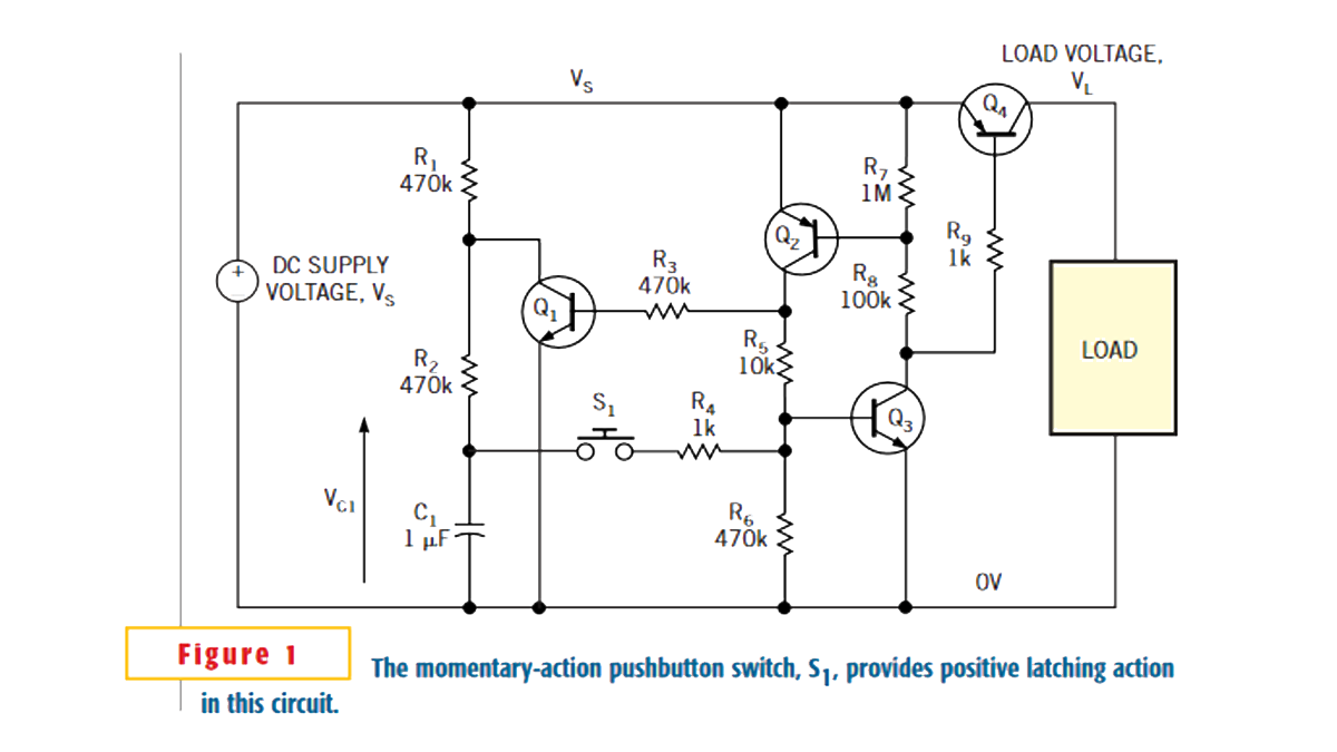
When you first apply the supply voltage, VS, all four transistors are off, and capacitor C1 charges via R1 and R2 until its voltage, VC1, is equal to VS. The circuit is now in its off, or unlatched, state, and the load voltage, VL, is 0V. A momentary closure of the pushbutton switch, however, causes C1 to dump its charge into the base of Q3, which conducts and furnishes bias for Q2 and Q4, which both turn on. Q2 now provides base bias for Q3 via R5, and also for Q1 via R3. The circuit is now in its on, or latched, state and remains that way even though S1 is open. The load is now energized, and VL is roughly equal to VS. Transistor Q1 is now saturated, causing C1 to discharge via R2 such that VC1 falls to a few tens of millivolts (Q1‘s collector-emitter saturation voltage). Another momentary closure of the pushbutton switch couples this low voltage to Q3‘s base, turning it off. As a result, all four transistors turn off, and the circuit reverts to its off, or unlatched, state. The load is now de-energized, and VL falls to 0V. Because Q1 is now off, C1 begins to charge again via R1 and R2, such that another momentary closure of S1 latches the circuit on again.
Timing capacitor C1, acting with R1 and R2, provides debouncing for the pushbutton switch, such that contact bounce has no effect on the desired latching function. Without the RC time delay, the circuit would “chatter” on and off each time you pressed the pushbutton switch and would end up in an indeterminate state. Although Figure 1 shows a value of 1 µF, other values may be more suitable for a particular application, so prepare to experiment. None of the resistor values is particularly critical, and the values shown in Figure 1 are fairly optimal for a supply voltage of approximately 1 to 1.5V—in other words, a single cell. At higher voltages, the resistor values should increase proportionally, although you should hold R2 and R4 constant at approximately 470 and 1 kΩ, respectively. Keeping the R2-C1 time constant fixed at a few hundred milliseconds ensures that the time taken to discharge the capacitor is not excessive; otherwise, once the circuit has been latched, there may follow an unacceptable delay before it can be unlatched. Resistor R4 limits the current flowing from C1 into Q3‘s base to a safe level; its value should be fairly small to ensure that R5 and R6 do not distort the voltage appearing at Q3‘s base when the switch closes.
Read more: Latching power switch uses momentary-action pushbutton
- Can a momentary pushbutton be used as a latching on/off switch?
Yes; the circuit uses a momentary SPNO pushbutton plus a four-transistor latch so a momentary press latches power on or off. - What role does C1 play in the circuit?
C1 provides debouncing and timing with R1 and R2, dumping charge to Q3 on press and discharging via Q1 when latched. - Which transistors form the latch?
Transistors Q2 and Q3 form an SCR-like structure that functions as the latch. - How is the load powered in the latched state?
Transistor Q4 switches power to the load, so when Q4 is on the load voltage VL is roughly equal to VS. - Can this circuit operate from a single cell?
Yes; the circuit can operate at voltages as low as about 1 V, making it suitable for single-cell applications. - How does the circuit unlatch?
A second momentary press couples the low C1 voltage to Q3's base, turning Q3 off and causing all four transistors to turn off, unlatching the circuit. - Are resistor values critical for different supply voltages?
Most resistor values are not critical; increase values proportionally at higher voltages but keep R2 about 470 Ω and R4 about 1 kΩ. - Why must R4 be fairly small?
R4 limits current from C1 into Q3's base and should be small enough so R5 and R6 do not distort the base voltage when the switch closes. - What happens to C1 after the circuit latches?
Q1 saturates and causes C1 to discharge via R2 so VC1 falls to a few tens of millivolts.