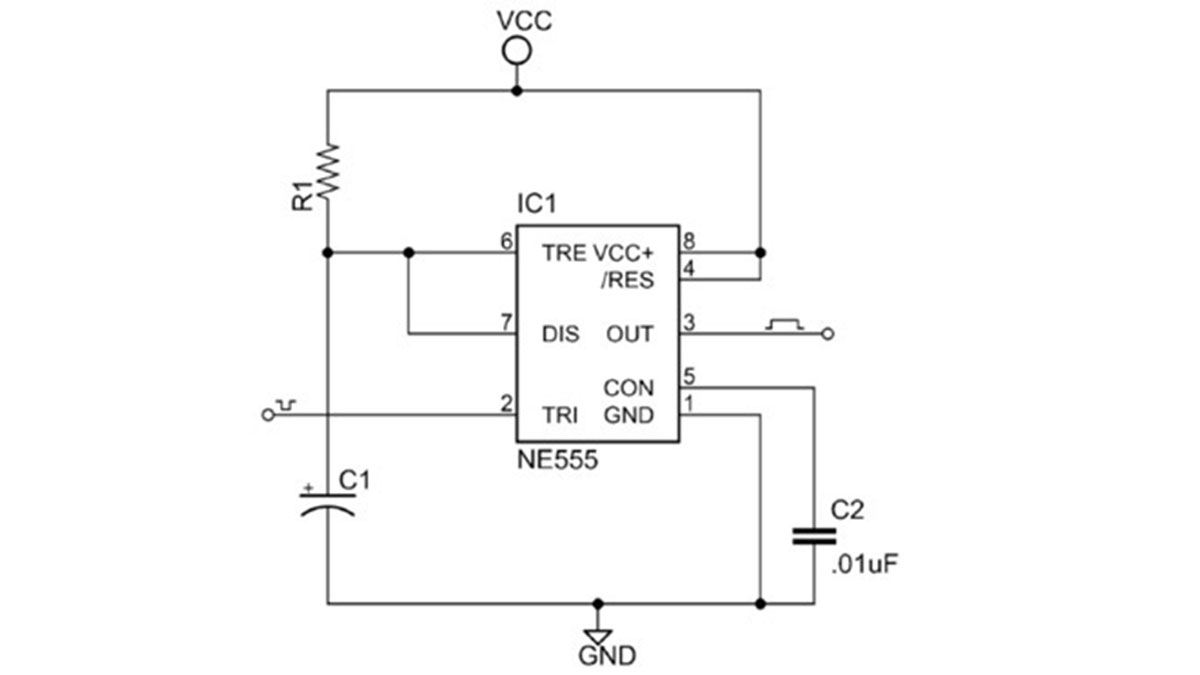
555 Signals and Pinout (8 pin DIP)
Figure 1 shows the input and output signals of the 555 timer as they are arranged around a standard 8 pin dual inline package (DIP).
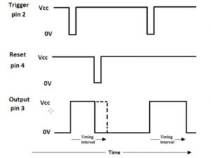
Pin 2 – Trigger (TRI)
A low voltage (less than 1/3 the supply voltage) applied momentarily to the Trigger input causes the output (pin 3) to go high. The output will remain high until a high voltage is applied to the Threshold input (pin 6).
Pin 3 – Output (OUT)
In output low state the voltage will be close to 0V. In output high state the voltage will be 1.7V lower than the supply voltage. For example, if the supply voltage is 5V output high voltage will be 3.3 volts. The output can source or sink up to 200 mA (maximum depends on supply voltage).
Pin 4 – Reset (RES)
A low voltage (less than 0.7V) applied to the reset pin will cause the output (pin 3) to go low. This input should remain connected to Vcc when not used.
Pin 5 – Control voltage (CON)
You can control the threshold voltage (pin 6) through the control input (which is internally set to 2/3 the supply voltage). You can vary it from 45% to 90% of the supply voltage. This enables you to vary the length of the output pulse in monostable mode or the output frequency in astable mode. When not in use it is recommended that this input be connected to circuit ground via a 0.01uF capacitor.
Pin 6 – Threshold (TRE)
In both astable and monostable mode the voltage across the timing capacitor is monitored through the Threshold input. When the voltage at this input rises above the threshold value the output will go from high to low.
Pin 7 – Discharge (DIS)
when the voltage across the timing capacitor exceeds the threshold value. The timing capacitor is discharged through this input
Pin 8 – Supply voltage (VCC)
This is is the positive supply voltage terminal. The supply voltage range is usually between +5V and +15V. The RC timing interval will not vary much over the supply voltage range (approximately 0.1%) in either astable or monostable mode.
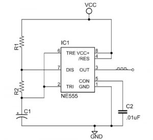
Monostable Circuit
Figure 2 shows the basic 555 timer monostable circuit.
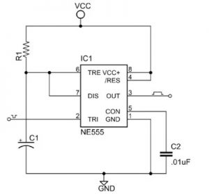
Figure 2: Basic 555 monostable multivibrator circuit.
Calculating the timing interval
Use the following formula to calculate the timing interval for a monostable circuit:
T = 1.1 * R1 * C1
Where R1 is the resistance in ohms, C1 is the capacitance in farads, and T is the time interval. For example, if you use a 1M ohm resistor with a 1 micro Farad (.000001 F) capacitor the timing interval will be 1 second:
T = 1.1 * 1000000 * 0.000001 = 1.1
Choosing RC components for Monostable operation
1. First, choose a value for C1.
(The available range of capacitor values is small compared to resistor values. It’s easier to find a matching resistor value for a given capacitor.)
2. Next, calculate the value for R1 that, in combination with C1, will produce the desired timing interval.
| R1 = | 1.1 * C1 |
Avoid using electrolytic capacitors. Their actual capacitance value can vary significantly from their rated value. Also, they leak charge which can result in inaccurate timing values. Instead, use a lower value capacitor and a higher value resistor.
For standard 555 timers use timing resistor values between 1K ohms and 1M ohms.
Monostable Circuit Example
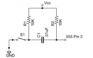
Figure 6 shows a complete 555 monostable multivibrator circuit with simple edge triggering. Closing switch S1 starts the 5 second timing interval and turns on LED1. At the end of the timing interval LED1 will turn off. During normal operation switch S2 connects pin 4 to the supply voltage. To stop the timer before the end of the timing interval you set S2 to the “Reset” position which connects pin 4 to ground. Before starting another timing interval you must return S2 to the “Timer” position.
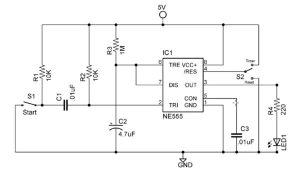
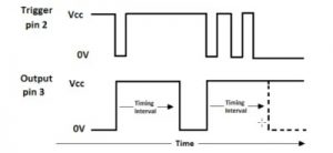
Figure 7 shows the basic 555 astable circuit.
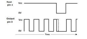
The timing diagram in figure 8 shows the 555 timer output in astable mode.
Calculating the period, frequency and duty cycle Figure 9 shows 1 complete cycle of a square wave generated by a 555 astable circuit.
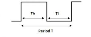
T = Th + Tl
where T is the period, in seconds.
You can calculate the output high and low times (in seconds) using the following formulas:
Th = 0.7 * (R1 + R2) * C1
Tl = 0.7 * R2 * C1
or, using the formula below, you can calculate the period directly.
T = 0.7 * (R1 + 2*R2) * C1
To find the frequency, just take the reciprocal of the period or use the following formula:
| f = | 1 | = | 1.44 |
Where f is in cycles per second or hertz (Hz).
For example, in the astable circuit in figure 7 if R1 is 68K ohms, R2 is 680K Ohms, and C1 is 1 micro Farad, the frequency is approximately 1 Hz:
| = | 1.44 (68000 + 2 * 680000) * 0.000001 | = 1.00 Hz |
The duty cycle is the percentage of time that the output is high during one complete cycle. For example, if the output is high for Th seconds and low for Tl seconds then the duty cycle (D) is:
| D = | Th Th + Tl | * 100 |
However, you really just need to know the values of R1 and R2 to calculate the duty cycle.
| D = | R1 + R2 R1 + 2*R2 | * 100 |
C1 charges through R1 and R2 but discharges through R2 alone so duty cycle will be greater than 50 percent. However, you can obtain a duty cycle very close to 50% by choosing a resistor combination for the desired frequency such that R1 is much smaller than R2.
For example if R1 is 68,0000 ohms and R2 is 680,000 ohms the duty cycle will be approximately 52 percent:
| D = | 68000 + 680000 68000 + 2 * 680000 | * 100 = 52.38% |
The smaller R1 is compared to R2 the closer the duty cycle will be to 50%.
To obtain a duty cycle that is less than 50% connect a diode in parallel with R2.
Choosing RC components for Astable operation
1. Choose C1 first.
2. Calculate the total value of the resistor combination (R1 + 2*R2) that will produce the desired frequency.
| (R1 + 2*R2) = | 1.44 f*C1 |
3. Select a value for R1 or R2 and calculate the other value. For example, say (R1 + 2*R2) = 50K and you select a 10K resistor for R1. Then R2 must be a 20K ohm resistor.
For a duty cycle close to 50%, select a value for R2 that is significantly higher than R1. If R2 is large relative to R1 you can initially ignore R1 in your calculations. For example, assume the value of R2 will be 10 times R1. Use this modified version of the above formula to calculate the value of R2:
| R2 = | 0.7 f*C1 |
Then divide the result by 10 or greater to find the value for R1.
For standard 555 timers use timing resistor values between 1K ohms and 1M ohms.
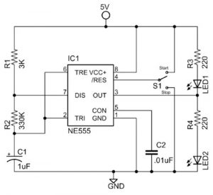
Astable Circuit Example
Figure 10 shows a 555 square wave oscillator with a frequency of approximately 2 Hz and a duty cycle of approximately 50 percent. When SPDT switch S1 is in the “Start” position the output alternates between LED 1 and LED 2. When S1 is in the “Stop” position LED 1 will remain on and LED 2 will remain off.
Low power versions
The standard 555 has a few characteristics that are undesirable for battery powered circuits. It requires a minimum operating voltage of 5V and relatively high quiescent supply current. During output transitions it produces current spikes of up to 100 mA. Additionally, its input bias and threshold current requirements impose a limit on the maximum timing resistor value, which limits the maximum time interval and astable frequency.
Low power CMOS versions of the 555 timer, such as the 7555, TLC555 and the programmable CSS555, were developed to provide improved performance, especially in battery powered applications. They are pin compatible with the standard device, have a wider supply voltage range (for example 2V to 16V for the TLC555) and require significantly lower operating current. They are also capable of producing higher output frequencies in astable mode (1-2 MHz depending on the device) and significantly longer timing intervals in monostable mode.
These devices have low output current capability compared to the standard 555. For loads greater than 10 – 50 mA (depending on the device) you will need to add a current boost circuit between the 555 output and the load.
For more information
Consider this a short introduction to the 555 timer. For further information be sure to study the manufacturers data sheet for the specific part that you are using. Also, as a quick Google search will verify, there is no shortage of information and projects devoted to this IC on the web. For example, the following web site provides more detail on both standard and CMOS versions of the 555 timer.