Summary of Basic knowledge of Zynq FPGA
Zynq is Xilinx’s all‑programmable SoC family combining dual-core ARM processors (PS) with FPGA fabric (PL) for high-performance, flexible embedded systems. Design flow involves task partitioning between PS and PL, hardware IP assembly, software development, and system integration. PS features include AXI interconnects, I/O (MIO/EMIO), memory interfaces, clocks, reset, DMA, IRQ, and APU components (FPU, NEON, MMU, caches). PL provides programmable logic (LUT/CLB), XADC, and configuration via PS. Zynq enables faster time-to-market, cost/power savings, improved performance, and easier interactive system programming.
Parts used in the Zynq Project:
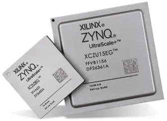
- Zynq-7000 SoC (APSoC with dual-core ARM Cortex-A9 and FPGA)
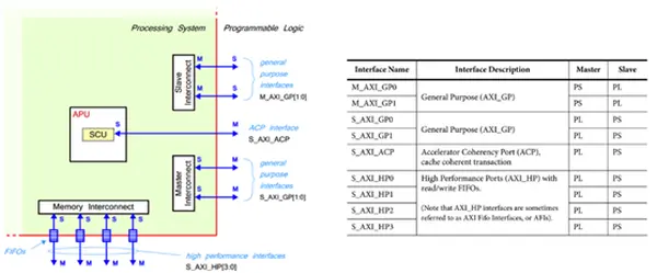
- AXI bus (AXI interfaces including ACP, High-Performance Ports, General-Purpose Ports)
- PS central interconnect
- MIO (Multiplexed I/O)
- EMIO (Extended I/O)
- Memory interfaces (static and dynamic)
- Clock generation module
- Reset module
- XADC (analog-to-digital conversion in PL)
- DMA (Direct Memory Access between PL and PS)
- IRQ (interrupt request mechanism)
- Config AES/SHA (FPGA configuration interface)
- APU components: FPU, NEON engine, MMU, I-Cache, D-Cache, 512KB L2 Cache, OCM (on-chip memory)
- PL programmable logic: CLBs, LUTs
Table of contents
1 What is the Zynq?
2 Design Flow of Zynq
3 PS (ARM)
4 How do I use Zynq?
5 Pros of Zynq
What is the Zynq?
The all-programmable Zynq-7000 SoC processor The next-generation all-programmablesystem-on-a-chip from Xilinx, called Zynq, combines the hardware and software programmability of an FPGA and a processor. System performance, adaptability, and scalability are all excellent. High-end embedded applications like video surveillance, automobile driver assistance, and factory automation are designed to require the processing power and computing performance. It is a SOC (System on Chip) chip, a system on a chip, and it has both an ARM CPU and a conventional FPGA. The AXI bus, PS (on the ARM side) and PL (on the FPGA side) serve as the interface for communication between FPGA and ARM. The PS side interface can be extended to the PL side using emio. RFSoC, or more properly, Zynq®Ultra- Scale+ RFSoC, is based on Xilinx’s prior family, the Zynq UltraScale+ MPSoC.
Zynq is an APSoC, which means that developers can use the FPGA, or field-programmable gate array, technology included in it in addition to integrating the majority, if not all, of a computer’s components into a single chip. FPGAs are often stand-alone devices that are used to create the hardware for future application-specific integrated circuits (ASICs) or prototype custom system chips. As a result, while referring to Zynq, the term “system” in APSoC refers to the system of two separate processors (Dual-core ARM Cortex-A9 Processors) and FPGA technology. The best of both worlds can be accessed by developers who have access to both processor and FPGA functions.
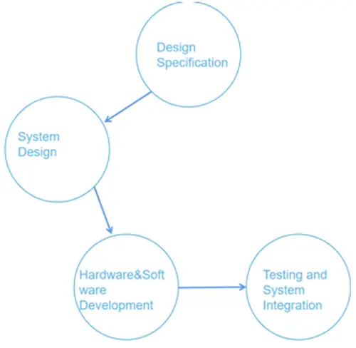
Design Flow of Zynq
There are several design flow phases that are similar to those of a standard FPGA for the Zynq architecture. Specifying the system’s needs and specifications is the initial step. The individual tasks (functions) are then assigned to implementation in either PL or PS during the system design stage, a process known as task partitioning. This phase is critical because it determines which activities or functions will be implemented using hardware or software, depending on the most appropriate technology.
The creation and testing of the hardware and software should come next. To achieve the design criteria, it is necessary to determine the functional blocks that must be present in the PL, as well as to put them together as IPs and connect them in the proper ways. Similarly, the software activity entails writing code for the PS. As a result, system integration and testing are necessary to finish the design.
PL (FPGA)
The logic of digital integrated circuits produced in the early days were fixed. To change its logical function, one must change the connections between the internal unit circuits, which are fixed during the IC production process.
Integrated circuits that allow users to modify their own internal connections: Programmable Logic Device (PLD). The internal circuit structure of PLD can be set by writing programming data. The programming data written to the PLD can also be erased and rewritten. Commonly used programmable logic devices:CPLD: Complex Programmable Logic Device (CPLD), FPGA: Field Programmable Gate Array (FPGA). The essence of the difference: the circuit structure is different.CPLD: Array of sum-or-sum logic based on “product terms. FPGA: CLB array based on “Look Up Table” (LUT)
PS (ARM)
3.1 PS
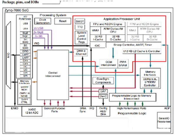
1.Central Interconnect: Terminal interconnect, responsible for managing and directing the communication between AXI interfaces.
2.I/O: Interface with the outside world, connected to the outside world through MIO. 54
3.Memory Interfaces: Memory interfaces, static (lower left) or dynamic (right) memory interfaces.
- Clock Generation: Clock generation module, generate the clock frequency required by each internal module.
5.Reset: reset module
PL terminal (the following part)
6.EMIO: Expansion IO, by connecting to the PL IO for expansion.
7.XADC: PL inside the hard core, to achieve digital-to-analog conversion.
8.DMA: PL to PS direct memory access.
9.IRQ: interrupt request, PL side can generate interrupts to pass to the PS interrupt controller.
10.Config AES/SHA: FPGA configuration interface. the PL part is actually configured by the PS. the PS starts configuring the PL first.
11.AXI interface: including ACP, High-Performance Ports Programmable Logic, General-Purpose Ports.
3.2 APU
1.FPU and NEON Engine: FPU floating point unit, NEON single instruction multi-data engine. Massive parallel computing acceleration.
2.MMU: storage management unit, physical address to virtual address mapping.
3.I-Cache, D-Cache: Instruction Cache and Data Cache. one level of Cache.
4.512KB L2 Cache: L2 Cache, shared by two processors.
5.OCM: on chip memory, on-chip memory
6.DMA: direct memory range, data transfer
7.GIC: interrupt controller
3.3 AXI
How do I use Zynq?
Compared to ASICs, ASSPs are less dangerous and may reach the market sooner. However, because it is a standard product, it has little design freedom. To achieve a fair trade-off, developers frequently choose to use a 2-chip system that combines an FPGA with an ASIC or ASSP. However, using two chips presents a completely new set of difficulties for programmers.
Zynq is distinctive in that it offers a solution for every issue mentioned above and does it successfully in a single chip, making it the first of its type. It gives FPGA hardware programmers access to the same resources that software programmers often have (such as Python programming languages, operating systems, drivers, etc.).
Without having to change the architecture of their applications, software developers can use Zynq to adapt and expand the functionality of their programs onto their hardware. Due to Zynq’s FPGA capacity to expand the peripheral capabilities of the dual ARM A9 processors, the same hardware design can be applied twice. Developers just need to change the elements of their design that must change with each iteration.
Pros of Zynq
| Pros of Zynq | |
| Quick Time to Market | Zynq provides developers with a significant productivity edge. Programmable logic’s adaptability enables manufacturers to create customized products without going through the time-consuming and expensive process of creating an ASIC. If specs change, designers can quickly alter the device both before the product is released and while it is being used.
|
| Cost and Power Savings | Zynq has the ability to combine features from several components into a single chip while still performing the intended function. Up to 40% in cost reductions may result from this. Zynq’s versatility enables users to use a single chip for a variety of products. |
| Improvements in System Performance | The integration of the bandwidth between the processing system and programmable logic is what distinguishes Zynq from other alternatives. This bandwidth is several orders of magnitude greater than what a 2-chip system would be able to provide. As a result, accelerators with up to a 10x increase in performance can be made to offload processing-intensive jobs. |
| Interactive Systems Programming | Zynq is a significant advancement in SoC-level integration. It combines, in a single device, the capabilities and power characteristics of an ASIC, the adaptability of an FPGA, and the programming simplicity connected to microprocessors. Compared to a 2-chip solution, Zynq is more dependable and secure because it is a fully integrated system. |
- What is the Zynq?
Zynq is an all-programmable SoC from Xilinx that combines dual-core ARM processors (PS) and FPGA fabric (PL) to provide both hardware and software programmability. - How does communication occur between PS and PL?
Communication between PS and PL uses the AXI bus and can be extended via EMIO. - What are the main phases in the design flow of Zynq?
Design flow includes specifying requirements, task partitioning between PL and PS, creating and testing hardware and software, then system integration and testing. - What components are included in the PS?
The PS includes a central interconnect, I/O (MIO), memory interfaces, clock generation, reset module, DMA, IRQ, and AXI interfaces. - What APU features does Zynq provide?
The APU includes an FPU, NEON engine, MMU, I-Cache, D-Cache, a shared 512KB L2 cache, OCM, DMA, and a GIC interrupt controller. - How is the PL configured?
The PL is configured by the PS using the FPGA configuration interface (Config AES/SHA), with the PS initiating configuration. - How does Zynq improve time to market?
Zynq’s programmable logic enables quick design changes without creating an ASIC, allowing faster adaptation before release and during use. - Can Zynq reduce cost and power?
Yes; by integrating multiple component functions into a single chip, Zynq can deliver cost reductions and versatility across products. - Does Zynq improve system performance compared to two-chip solutions?
Yes; integrated bandwidth between PS and PL is orders of magnitude higher than a 2-chip system, enabling accelerators up to 10x faster for intensive tasks. - How does Zynq benefit software developers?
Zynq lets software developers expand functionality into hardware without changing application architecture, using familiar software resources like operating systems and drivers.