Summary of A 400W (1kW Peak) 100A Electronic Load Using Linear MOSFETs
This article details a high-performance electronic load project utilizing two IXYS IXTK90N25L2 linear MOSFETs to achieve over 100A current sinking and 400W continuous dissipation. The design employs parallel channels with low-resistance shunt feedback, requiring precision opamps due to minimal voltage drops. Constructed on protoboards mounted to a polished aluminum heatsink, the circuit uses heavy-gauge wiring and copper cladding to manage high currents effectively.
Parts used in the 100A Electronic Load:
- Two IXYS IXTK90N25L2 linear MOSFETs
- Two 50A/75mV current shunt resistors (1.5mΩ each)
- Precision operational amplifiers (opamps)
- Krohn-Hite MV216A voltage standard
- Large aluminum block heatsink
- 2oz copper clad board material
- 6 AWG equivalent wires
I bought a couple of IXYS linear MOSFETs (IXTK90N25L2) a while ago to test their capabilities when used as electronic load, and the result was quite impressive. So I decided to build another electronic load using both MOSFETs. As you can see in the video towards the end, this electronic load can sink more than 100 Amps of current while dissipating more than 400W continuously and can withstand more than 1kW of power dissipation in pulsed operation mode.
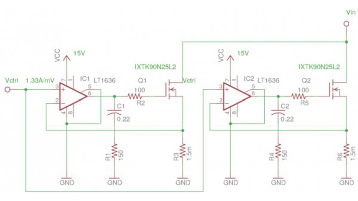
The circuit is almost identical to the one I used in my previous experiments. Instead of using a single MOSFET, two MOSFETs are used. Each channel is identical. When the voltage control inputs and the drains of the MOSFETs are tied together, the load is essentially divided equally between the two MOSFETs. I used two 50A/75mV current shunt resistors as the feedback resistors. The obvious benefit in choosing such small resistance value (each shunt is only 1.5mΩ) is that the voltage drop is virtually negligible. Even when handling an 100A load, the voltage drop across each shunt resistor is only going to be 75mV.
The downside of using such low valued shunt resistors is that it requires the opamps to have extremely low input offsets as even a small offset can introduce a large error in controlled drain-to-source current. For instance for my particular setup, a 100µV offset voltage would cause a 133mA change in the load current. Also, it is difficult to generate such low and stable control voltages without using precision DACs and precision opamps. My intention was to use this electronic load with my Krohn-Hite MV216A voltage standard so generating a low and stable control voltage is not an issue (MV216A has a voltage resolution of 0.1µV in the mV range). If you plan to use a microcontroller to control the load like I did in my previous electronic load build, you will need to either use precision opamps to amplify the shunt voltages to a range that is compatible to your DAC’s output (e.g. 0-5V) or use a low tempco precision voltage divider to generate the mV range control signal.
The entire circuit was built on protoboards and placed on top of a large aluminum block. The surface of the aluminum block was polished slightly to ensure good thermal conduction between the TO-264 package and the heatsink. 2oz copper clad was used for higher current carrying capabilities in the high current portion of the circuit. All the wiring on the main current path are done using at least 6 AWG equivalent wires to ensure that they can handle at least 100A without significant heat-up or voltage drop.
Read more: A 400W (1kW Peak) 100A Electronic Load Using Linear MOSFETs
- How much current can this electronic load sink?
The load can sink more than 100 Amps of current. - What is the continuous power dissipation capability?
The device dissipates more than 400W continuously. - Can the load handle pulsed power operation?
Yes, it can withstand more than 1kW of power dissipation in pulsed mode. - Why were 1.5mΩ shunt resistors chosen for this project?
They ensure the voltage drop remains virtually negligible even at high loads. - What component provides the stable control voltage?
A Krohn-Hite MV216A voltage standard is used to generate precise control signals. - How are the two MOSFETs connected in the circuit?
Their voltage control inputs and drains are tied together to divide the load equally. - What material is used for the high current paths to prevent heat-up?
At least 6 AWG equivalent wires are used for all main current path wiring. - Why was the aluminum block surface polished?
Polishing ensures good thermal conduction between the TO-264 package and the heatsink.