Summary of Will Silicon Substrates Push LED Lighting Into the Mainstream?
This article discusses the shift toward silicon substrates for LEDs to reduce costs and improve manufacturing efficiency. Unlike traditional sapphire or silicon-carbide (SiC) substrates, silicon offers larger wafer sizes (8 inches vs. 4 inches), compatibility with existing CMOS fab capacity, and simplified dicing processes. These advancements aim to overcome historical issues like crystal lattice mismatches that caused defects in earlier silicon-based attempts, potentially making LED lighting affordable enough to replace incandescent bulbs.
Parts used in Silicon-Substrate LED Manufacturing:
- Gallium nitride (GaN)
- Silicon substrate
- Sapphire substrate
- Silicon-carbide (SiC) substrate
- Yttrium aluminum garnet (YAG) phosphor
- CMOS IC technology
- Epitaxy layers
- p-contact
- n-contact
By Steven Keeping, Electronic Products
9/24/2013
LEDs have many advantages over traditional lighting including efficacy, longevity, and robustness, but price is not one of them.
The reason why LEDs are expensive is partly because the manufacturing process used to fabricate the wafers from which the individual chips are cut is difficult and employs exotic materials such as gallium nitride (GaN) deposited on sapphire or silicon-carbide (SiC) substrates.
But recently, some manufacturers have proposed using silicon, the material routinely used to fabricate billions of integrated circuits (ICs) every year, as an LED substrate. Apart from potentially reducing the cost of LEDs, the use of mature complementary metal oxide semiconductor (CMOS) IC technology would allow fabrication in conventional wafer fabs that have spare capacity.
However, the idea is not new. Silicon has been tried before, but large mismatches between its crystal structure and coefficient of thermal expansion, and those of the GaN used for the LED proper created faults that lowered the end product’s efficacy and dramatically shortened its life. Now new developments promise to overcome these drawbacks.
This article describes recent advances in manufacturing technology for silicon-substrate LEDs with reference to the work done by major makers, and compares the performance of the experimental chips with today’s commercial LEDs.
Substrate wars
“White” LEDs, typically blue LEDs working in conjunction with yttrium aluminum garnet (YAG) phosphor (see the TechZone article “Whiter, Brighter LEDs”), used for lighting applications have only been commercially produced for two decades, and as such the technology can be said to be still in its infancy.
A commercial white LED like Philips Lumileds’ Luxeon T chip, a device that produces 111 lm/W at 700 mA, exemplifies the state-of-the-art in solid-state lighting. Further gains in efficacy are likely, as Philips Lumileds and others major suppliers such as OSRAM and Cree continue to develop their products.
Efficacy has risen from 15 lm/W in 2000 to around 200 lm/W for devices currently on the lab bench. In the same timeframe, the price of a group of white LEDs required to generate 1,000 lm has dropped from $302 to $7.
Despite these impressive gains, LEDs are still too expensive for most consumers as a replacement for traditional lighting. An LED-based luminaire that can be screwed into a standard light socket is about 15 times as expensive as an incandescent bulb, and 5 times the cost of a compact fluorescent light (CFL). Nonetheless, in 2011, LEDs made up around 12.3 percent of the global lighting market and are predicted to rise to over 64 percent by 2020 (Figure 1).
But before this forecast becomes reality, manufacturers need to bring down the cost of LED lighting to near parity with existing technologies.
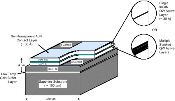
Today, the majority of LEDs are constructed from a combination of GaN, which features a band gap suitable for emitting photons in the visible part of the spectrum, and sapphire substrate. GaN thin films are grown by a process known as epitaxy, which builds up the LED’s active regions, the multiple layers sandwiched between the p- and n-contact, by depositing successive layers on the substrate. A simplified schematic of the structure of one type of commercial high-brightness LED is shown in Figure 2.
A key disadvantage of sapphire substrate is the relatively large mismatch between the crystal lattice of GaN and the sapphire itself. The mismatch results in microscopic flaws in the GaN thin film, known as threading dislocations, which affect both LED luminosity and lifetime.
This has led to the rise of SiC as an alternative substrate. SiC has a crystal structure that is much more closely matched to GaN than sapphire, reducing the defect density, and improving efficacy and longevity, by at least one and sometimes two orders of magnitude.2 (See the TechZone article “Material and Manufacturing Improvements Enhance LED Efficiency.”)
Another problem with both sapphire and SiC is that they are expensive to produce. Worse yet, the material can only be manufactured on wafers typically measuring 4 in. in diameter (although some fabricators such as OSRAM now produce 6 in. wafers).
Some manufacturers have suggested that a cheaper production technique could be to grow LEDs on larger silicon wafers. Silicon is the mainstay of the chip fabrication industry, and foundries are well versed in producing high-yield, high-volume 8 in. wafers for IC manufacture. If silicon could be used as a substrate for the GaN epitaxy process, the price of LEDs should fall.
A 4 in. wafer has a surface area of around 12.6 in.², compared to an 8 in. wafer’s surface area of over 50 in.². Because it takes almost as long to process a 4 in. wafer as it does a 6 in., the same factory could quadruple production by switching to the larger size with little increase in cost.
Moreover, using current manufacturing techniques, sapphire or SiC wafers are diced into individual devices before testing and packaging. Silicon lends itself to a shorter dicing operation because a manufacturer could leave 16 or 32 LEDs together in a unified block, and subsequently test and package as a single device. The packaging and testing phase account for close to 35 percent of the cost of manufacturing today’s LEDs, so single packages comprising multiple dies would further drive down unit costs, while increasing throughput.3
For more detail: Will Silicon Substrates Push LED Lighting Into the Mainstream?
- Why are LEDs currently expensive?
LEDs are expensive because their manufacturing process uses difficult fabrication methods and exotic materials like gallium nitride deposited on sapphire or silicon-carbide. - How does using silicon as a substrate reduce LED costs?
Using silicon allows for larger 8-inch wafers instead of smaller 4-inch ones and leverages mature CMOS technology in foundries with spare capacity. - What problem did early silicon-based LEDs face?
Early attempts failed due to large mismatches between the crystal structure and thermal expansion coefficients of silicon and gallium nitride, causing faults. - What is the role of YAG phosphor in white LEDs?
White LEDs typically use blue LEDs working in conjunction with yttrium aluminum garnet phosphor to produce light. - How does silicon improve the dicing and packaging process?
Manufacturers can leave multiple LEDs together in a unified block on silicon wafers, allowing them to be tested and packaged as a single device to lower costs. - What is the current efficacy trend for LEDs?
Efficacy has risen from 15 lm/W in 2000 to around 200 lm/W for devices currently being developed in labs. - Why is SiC considered better than sapphire for substrates?
SiC has a crystal structure much closer matched to GaN than sapphire, which reduces defect density and improves efficacy and longevity. - What percentage of the global lighting market did LEDs hold in 2011?
In 2011, LEDs made up approximately 12.3 percent of the global lighting market.