Summary of What is a Printed Circuit Board?
PCB design turns electronic circuits into physical boards and requires careful decisions on size, layers, materials, and manufacturing steps. Key considerations include product constraints, layer count (which affects complexity and cost), material selection, and adherence to standards. Manufacturing involves design, printing, substrate creation, etching (chemical, wet, dry), lamination, plating, solder mask, surface finish, and testing. PCBs consist of laminate, prepreg, copper foil, nomenclature, solder mask, and final finish, plus components like resistors, transistors, capacitors, inductors, transformers, and sensors. Proper process adherence ensures reliable board performance.
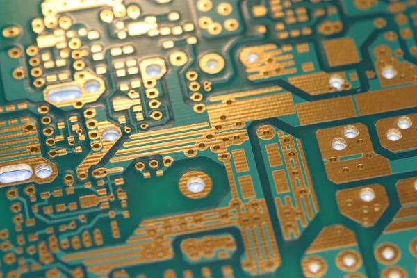
Parts used in the PCB Design and Manufacturing Project:
- Laminate
- Prepreg
- Copper foil
- Nomenclature
- Solder mask
- Final finish
- Resistors
- Transistors
- Capacitors
- Inductors
- Transformers
- Sensors
A printed Circuit board or PCB is a non-conductive material with various conductive lines etched or printed. Electric components are mounted on the board, and traces attach the components to create a working circuit.
But before you come up with a PCB, you need to start with a design. PCB design brings the electronic circuits to life. However, designing a PCB is not an easy task. There are several steps to go through. Hence, there is a lot about the process you need to know.
Below are vital things you need to know before starting PCB design
Things You Should Know before Starting PCB design
1. PCB Size
PCB size depends on various factors. For instance, the size of your product will determine the size of the PCB. Some factors that determine the PCB size include copper width, design complexity, component density, and matching impedance requirements.
2. PCB Layer
Before starting PCB design, the important thing you need to know is the PCB layer. You need to note that the more layers you have, the more complex the manufacturing of your PCB will be.
In addition, the more layers a PCB has, the more costly it is to manufacture. PCBs with two layers are for simple products such as toy products, PCBs with four layers are for average products, and those with six, eight or more layers are for complex products such as smartphones.
3. PCB Material
PCBs use a wide range of materials as components and substrates. Hence, material selection is based on the requirements of the application. This is because different materials offer differing circuit qualities.
PCB designers select materials based on the electrical performance of the application. In addition, designers need to comply with government requirements.
The main components of a normal PCB are:
*Laminate
*Prepreg
*Copper foil
*Nomenclature
*Solder mask
*Final finish
PCB manufacturing
PCB manufacturing goes through a complex procedure that ensures the final product’s performance is of high quality. Even though PCBs can be single-sided, double-sided, or multilayer, the manufacturing process only differs after the first layer.
There are several steps needed when manufacturing a PCB. Missing any step can negatively affect the performance of the board. But when completed successfully, the PCBs can perform their tasks properly.
PCB constituents
PCBs are made up of various electrical constituents, where each one plays a vital role to make sure the device is running smoothly. Keep in mind that if one constituent fails, the whole board will not work properly.
Some of the PCB components are:
*Resistors – some of PCBs’ most common and vital constituents are resistors. Their work is to transmit an electrical current to produce a voltage and disperse electrical power as heat.
*Transistors – it is an amplifier that controls the electrical signals in the PCB. The common transistor has three pins (the base, collector, and emitter)
*Capacitors – they work is to hold an electrical charge within the printed circuit board and release it when more power is needed.
*Inductors – they store energy and are used to block signals within the printed circuit board. *Transformers – they are to transfer the electrical energy from one circuit to the other by a decrease or an increase.
*Sensors – sensors are elements that sense changes in the environment to respond to signals that correspond with the changes.
Chemical Etching
Chemical etching is one of the main steps of PCB manufacturing. It is a subtractive method that is mostly used on metal. In the process, metal is removed to create metal parts in desired thickness and shape.
The procedure involves bathing the PCB material into a corrosive chemical, reacting to areas that need to be removed.
Photographic process
Even though PCBs are manufactured through several manufacturing processes, the photographic process is common. It is mainly used to help gain the correct pattern of the tracks.
The copper on the printed circuit board is covered with a very thick layer of photoresist in the photographic process. Later, it is exposed to light through a photo mask or photographic film detailing the tracks needed.
Placing PCBs in Etch
PCB etching is a process of careful removal of materials from the outer layer of the PCB. It is also known as cleaning out conductive materials that are in excess. There is wet etching and dry etching.
*Wet etching – this is where the copper layers are dipped into the etching chemical fluid. It is a popular method because it does not change the properties.
*Dry etching – also known as plasma etching, is where a machine is used to remove leftover residues. The process is less stressful and a good option for a large volume of PCB production.
PCB etching is a vital process in the PCB manufacturing process. However, it can be very tasking, especially for a beginner. Hence, it is essential to know how it works to help you achieve the expected results.
There is DIY PCB etching where you can decide to handle the process at home. However, you need to follow every step and need elements to fabricate a PCB. This is something you can do at home or in the laboratory.
Other methods of manufacturing
Even though PCBs are small, the manufacturing process is extensive. It does not matter whether it is a DIY manufacturing process or through a PCB factory. You need to go through all the needed steps to have a great finished product.
The main steps of PCB manufacturing include the design, printing the design, creating substrate, removing unwanted copper with CNC machining, laminating of layers, plating, etching, solder mask application, surface finish, and testing.
Summary
The PCB manufacturing process is a vital element of modern electronics production. It has enabled significant improvements in many devices across various sectors.
Understanding what you need to know before starting a PCB design is very important. In addition, you need to know the steps and why every step must occur. This will give you better know-how of the costs and the effort you need to put into each PCB
- What determines PCB size?
PCB size is determined by product size, copper width, design complexity, component density, and matching impedance requirements. - How does layer count affect PCB design?
More layers increase manufacturing complexity and cost; two layers suit simple products, four layers for average products, and six or more for complex products. - What factors influence PCB material selection?
Material selection is based on application requirements, electrical performance needs, and compliance with government requirements. - What are the main components of a normal PCB?
The main components are laminate, prepreg, copper foil, nomenclature, solder mask, and final finish. - What are common PCB constituents or components?
Common components include resistors, transistors, capacitors, inductors, transformers, and sensors. - What is chemical etching in PCB manufacturing?
Chemical etching is a subtractive method where corrosive chemicals remove metal to form desired shapes and thicknesses. - How does the photographic process help in PCB manufacturing?
The photographic process uses photoresist and a photo mask or film to produce the correct track pattern on copper. - What is the difference between wet etching and dry etching?
Wet etching dips copper in chemical fluid and preserves properties, while dry etching (plasma etching) uses machines to remove residues and suits large volumes. - Can PCB etching be done at home?
Yes, there is a DIY PCB etching process, but it requires following every step and having the necessary elements for fabrication. - What are the main steps of PCB manufacturing?
Main steps include design, printing the design, substrate creation, CNC removal of unwanted copper, lamination, plating, etching, solder mask application, surface finish, and testing.