3d

3D IMAGE SENSOR REAL3 FOR FACE AUTHENTICATION ANNOUNCED AT CES 2020

3D IMAGE SENSOR REAL3 FOR FACE AUTHENTICATION ANNOUNCED AT CES 2020

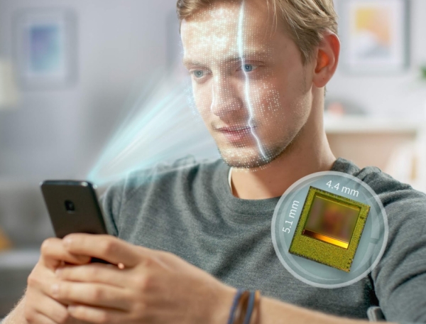
Infineon Technologies AG has collaborated with software and 3D Time-of-Flight (ToF) system specialist pmdtechnologies ag to develop reportedly the world’s smallest, most powerful 3D image sensor. Designated the REAL3, the single-chip solution measures just 4.4 x 5.1 mm and is the fifth generation of time-of-flight deep sensors from Infineon. The sensor can be incorporated into even the smallest devices with just

3D IMAGE SENSOR REAL3 FOR FACE AUTHENTICATION ANNOUNCED AT CES 2020 Continue Reading

RESEARCHERS EXPAND MICROCHIP CAPABILITY WITH NEW 3D INDUCTOR TECHNOLOGY

RESEARCHERS EXPAND MICROCHIP CAPABILITY WITH NEW 3D INDUCTOR TECHNOLOGY

Smaller is better when it comes to microchips, researchers said, and by using 3D components on a standardized 2D microchip manufacturing platform, developers can use up to 100 times less chip space. A team of engineers has boosted the performance of its previously developed 3D inductor technology by adding as much as three orders of

RESEARCHERS EXPAND MICROCHIP CAPABILITY WITH NEW 3D INDUCTOR TECHNOLOGY Continue Reading

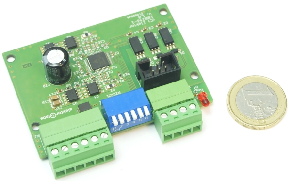
FREE ELEKTOR ARTICLE TMC2160 MOTOR DRIVER BOARD

FREE ELEKTOR ARTICLE: TMC2160 MOTOR DRIVER BOARD

Stepper motors are popular in computer and microcontroller-based position control applications like robotics, industrial automation, CNC machines, 3D printers and video camera control. Due to their uncomplicated internal construction and their limited number of connection wires, stepper motors look deceptively simple. On the internet, there are even lots of tutorials on how to control these

FREE ELEKTOR ARTICLE: TMC2160 MOTOR DRIVER BOARD Continue Reading

SAMSUNG UNVEILS 12 LAYER 3D TSV CHIP PACKAGING TECHNOLOGY

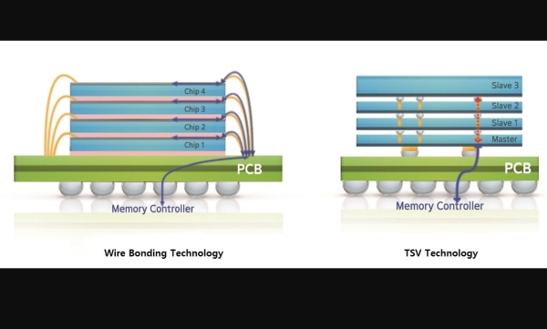
SAMSUNG UNVEILS 12-LAYER 3D-TSV CHIP PACKAGING TECHNOLOGY

An industry’s first, the 12-layer 3D-TSV (Through Silicon Via) technology developed by Samsung Electronics enables the stacking of 12 DRAM chips using more than 60,000 TSV holes, while maintaining the same thickness as current 8-layer chips. By Julien Happich @ eenewseurope.com Developed for the mass production of high-performance chips, the layered packaging technology requires pinpoint accuracy

SAMSUNG UNVEILS 12-LAYER 3D-TSV CHIP PACKAGING TECHNOLOGY Continue Reading

Scroll to Top