Vision
The aim of our project is to be able to control a electrical switching process using a remote. The idea is to come up with an alternative to the conventional electric switch boards, using a wireless control mechanism, in an economic way. In other words, an Electric Switch Board is to be designed in which the switching is controlled by a remote. These kind of switchboards could replace the old ones and used for controlling household appliances and any other devices.
Basic Outline
The control mechanism could be either RF based or IR based. We have decided that our project should be RF based as it has many advantages like long range, no requirement of LOS(Line Of Sight).We chose the RX434 and TX434 modules for the wireless transmission of data.
Formulation of the Problem
Transmitter Circuit
The transmitter should be able to perform two functions. It should inform the receiver that a switch has been pressed and transmit the information regarding which switch is pressed. This can be achieved by transmitting 4 bits. One HIGH bit and three address bits to distinguish between eight different switches. So, the transmitter circuit should transmit 4 bits.
But, the capability of the RF transmitter limit us to send only one bit at a time. So, we should transmit one bit at a time. This is achieved by using a multiplexer. A one of four multiplexer with the first bit connected to HIGH is to be used for the task. The multiplexer requires an address to select which bit is to be transmitted. Since there are four bits to be distinguished, a two bit address is sufficient.
For this task, we can use a modulo four counter, which is essentially a combination of two d flip-flops. The counter requires a clock. The clock can be generated using a 555 timer in astable mode. The three bits regarding the information about the switch pressed is generated using a 8-3 encoder. The eight switches are to be connected to the encoder inputs which encodes the information regarding the switch pressed.
Thus our transmitter can summarized as the following block diagram.
This block diagram illustrates the design and working of the transmitter circuit. The important components are:
1.Fixed width Pulse Generator
2.Clock Generator
3.Modulo 4 Counter
4.8 to 3 Encoder
5.1 0f 4 Multiplexer
6.RF Transmitter
The fixed width pulse generator (FWPG) generates a high pulse on required time period chosen. The FWPG is triggered at the press of any button. This pulse is fed as the Vcc for the rest of the circuit elements. This also ensures that the static power dissipation is minimum. The next component is the Clock Generator, which generates the clock, whose time period is one-fourth of the pulse of the fixed width pulse generator. This clock is fed to the Modulo four counter which cycles through the four addresses at the negative end of the clock. This two bit address is provided to the multiplexer, whose first bit is connected to HIGH. The remaining three inputs are the outputs of the 8 to 3 encoder, which encodes the information regarding the switch pressed into three bits. The multiplexer selects one bit at a time corresponding to the address provided and this is fed to the RF transmitter and transmitted through the antenna.
Receiver Module
It is time that we analyze the RF transmitter and receiver now. The receiver has a normal floating voltage of around 1.7 V if the transmitter is inactive. When a HIGH bit is transmitted, an instant high PULSE is generated for a short moment and the value settles at LOW till the transmission is stopped at the Transmitter. If we analyze the output of the receiver closely we observe many noise spikes also. So, we cannot really rely on this small HIGH pulse. So, we should conclude our HIGH bit based on the LOW state of the receiver.
We are going to use Arduino UNO in the receiver module. The algorithm is basically as follows: We continuously analog read the output at the RF receiver and wait for a HIGH output and then if confirm if it is due to real transmission and not a noise spike. After this, the next three bits are to be read by the micro-controller. The three bits read from the receiver give the information about the switch pressed. This is decoded accordingly and electric load is to be toggled. The electric load can be controlled by using Relays. So, the loads are connected to the relays which are driven by the Arduino through L293D drivers, as the relays require large currents.
Thus the receiver module can be summarized as a block diagram as below:
Design
Design of the Transmitter
Now it is time for the design of the final schematic of the transmitter
The only change in the schematic is the inclusion of L293D, which is done because the 555 timer cannot drive the current required for all the components of the circuit. The ICs used for the different components are:
1.NE555P for both Fixed width pulse generator and Clock Generator
2.L293D for the driving the current load
3.74HC112 for the modulo 4 counter
4.74LS148 for the 8-3 Encoder
5.74ACT153 for the 1 of 4 Multiplexer
The values of the resistors and capacitors used are:
C1 = C3 = 10nF
C2 = C4 = 10uF
R1 = 44KOhms
R2 = R3 = 5KOhms
Width of the Pulse generated by the FWPG = 1.1 x R1 x C2 = 484ms
Time Period of the Clock = ln(2)*(R2+R3)*C4 + ln(2)*(R3)*C4 = 104ms
Thus the transmission of four bits can be completed within the duration of the pulse.
The final circuit after assembling and soldering is as shown below:
To this transmitter the switches are attached and serves as the remote for Switching the electric loads.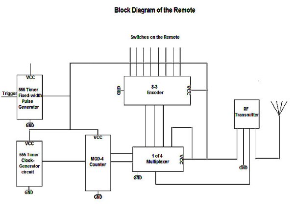
Design of the Receiver
As described earlier, the Arduino board cannot drive the current required by the relays. So, the relays are driven by the current from the L293D IC’s. The Arduino requires a 12 V source and the relays run at 6V. So, we used a 12V mobile charger to convert the 220V ac to 12V dc and feed the Arduino. We used a 7806 IC for clipping the DC Voltage at 6V for feeding through the current driver IC L293D.
The electric loads are to be connected across the LOAD terminals of the relays. AC main power should be supplied across the live and the neutral lines. This is the final schematic of the receiver module. The AC power itself is used for powering the relays and the micro-controller sparing us the cost of the battery, if used.
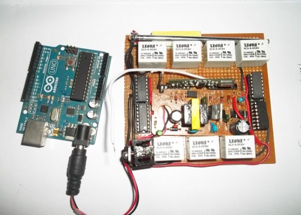
The final Receiver module after assembling and soldering is shown below:
The output of the RF Receiver is connected to the Arduino pin for analog reading and further processing to identify the switch pressed at the transmitter and activate the corresponding relay. There is a small problem regarding this. If the Arduino reads as accidental noise spike as a false alarm for the data transfer, it reads the next three bits as LOW since nothing is being transmitted (this is one of the drawbacks of this RF module).So, to avoid false toggling of the switches, we reduce the number of switches to seven and remove the switch corresponding to the 000 code and never use it. This is the reason for using only seven relays in the receiver. Thus, our remote can operate 7 different loads.
For more detail: Remote Controlled Switching