
Summary of KIOXIA UNVEILS FIFTH-GENERATION BICS FLASH
KIOXIA Europe has developed its fifth-generation BiCS FLASH 3D memory featuring a 112-layer vertical stack. This technology offers 512 Gb (64 GB) capacity using TLC, targeting mobile devices, SSDs, 5G networks, AI, and autonomous vehicles. It improves cell density by 20%, reduces cost per bit, and boosts interface speed by 50% compared to the previous 96-layer generation. Future plans include scaling to 1 Tb TLC and 1.33 Tb QLC devices.
Parts used in the Fifth-Generation BiCS FLASH:
- 112-layer vertically stacked structure
- Triple-level cell (TLC) technology
- Advanced circuit manufacturing process
- Silicon wafer
New generation 3D flash memory adds layers, boosts capacity, broader bandwidth and provides new design flexibility
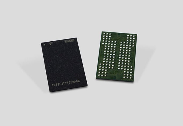
KIOXIA Europe GmbH, the world leader in memory solutions, today announced that it has successfully developed its fifth-generation BiCS FLASH three-dimensional (3D) flash memory with a 112-layer vertically stacked structure. KIOXIA plans to start shipping samples of the new device, which has a 512 gigabit (64 gigabytes) capacity with 3-bit-per-cell (triple-level cell, TLC) technology, for specific applications in the first quarter of the calendar year 2020[1].
The new device aims to fulfill ever-growing bit demands for a wide variety of applications, including traditional mobile devices, consumer and enterprise SSDs, emerging applications enabled by the new 5G networks, artificial intelligence and autonomous vehicles.
Going forward, KIOXIA will apply its new fifth-generation process technology to larger capacity devices, such as 1 terabit (128 gigabytes) TLC and 1.33 terabit 4-bit-per-cell (quadruple-level cell, QLC) devices.
KIOXIA’s innovative 112-layer stacking process technology is combined with advanced circuit and manufacturing process technology to increase cell array density by approximately 20 percent over the 96-layer stacking process. The new technology reduces the cost per bit and increases the manufacturability of memory capacity per silicon wafer. Additionally, it improves interface speed by 50 percent and offers higher programming performance and shorter read latency.
Since announcing the world’s first[2] prototype 3D flash memory technology in 2007, KIOXIA has continued to advance the development of 3D flash memory and is actively promoting BiCS FLASH to meet the demand for larger capacities with smaller die sizes.
Read more: KIOXIA UNVEILS FIFTH-GENERATION BICS FLASH
- What is the capacity of KIOXIA's new fifth-generation device?
The new device has a 512 gigabit or 64 gigabytes capacity. - How many layers does the new 3D flash memory have?
The device features an 112-layer vertically stacked structure. - Does the new technology improve interface speed?
Yes, it improves interface speed by 50 percent over the previous generation. - Can this memory be used for artificial intelligence applications?
Yes, the device aims to fulfill demands for applications including artificial intelligence and autonomous vehicles. - How much did the cell array density increase compared to the 96-layer process?
The new technology increases cell array density by approximately 20 percent. - What type of cells are used in this specific 512 Gb device?
This device uses 3-bit-per-cell triple-level cell technology. - Are larger capacity devices planned for future production?
Yes, KIOXIA plans to apply the technology to 1 terabit TLC and 1.33 terabit QLC devices. - When did KIOXIA first announce a prototype 3D flash memory technology?
KIOXIA announced the world's first prototype 3D flash memory technology in 2007.
