A Wifi platform for $3… who wouldn’t want to play with it?
For the last few weeks we have been seeing a lot of awesome projects built around ESP8266 Wifi modules:
These modules come in different shapes and colours and can be purchased from the internet for 3 dollars only.
They are therefore cheap enough to enable many Internet of Things applications like monitoring your home temperature and activity all year round (if you ever need to do that).
And at this price, you’re actually better off directly soldering the complete board on your existing PCB rather than integrating each of its components, as it would result in a higher board cost (for less than 10k platforms produced) and possible RF related problems.
The ESP8266 modules come with a pre-loaded firmware that will accept some commands through their UART interface (connect to wifi, open udp socket, send data to this IP…). Moreover, since Espressif recently released their SDK you can now load your own custom programs using the existing bootloader. To launch this bootloader you just have to connect some IOs to GND in a specific order.
However, anyone wanting to develop a project involving dozens of Wifi nodes has to start from somewhere, eg make a prototype of their future platform. That is why I developed this development board, so the prototyping stage is as simple as possible.
As you can see in the picture below the dev board breaks out all the ESP8266-03 IOs, includes a 3.3V LDO, a USB to UART converter, some logic and a button to automatically start the bootloader.
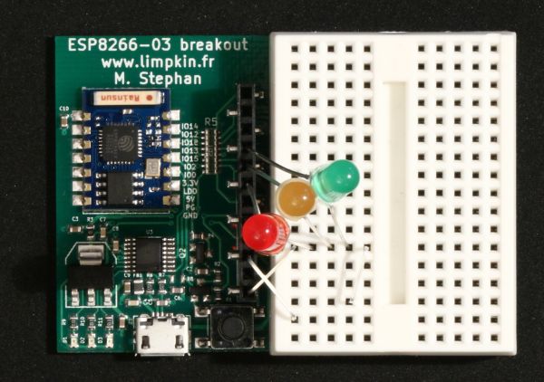
With the included breadboard solder free prototyping is therefore made possible!
You’ll notice that there aren’t any through hole components, so you may put double sided tape on the board’s back if you need to stick it somewhere. Have a look at the extremely simple schematics:
The LDO can provide up to 1A which is more than enough for the ESP8266 that supposedly needs around 230mA max.
Let’s talk about the “bootloader logic”. The exact sequence to launch the esp8266 in bootloader mode is to connect CH_PD to GND, connect GPIO0 to GND and finally release CH_PD to 3.3V while GPIO0 is still low.
The SW1 switch is directly connected to CH_PD with a pull-up to 3.3V. When it is not pressed no current flows through the P-Mosfet Q1 and the Q2 N-Mosfet gate is at 0v because of C2 leakage current. This is why the ESP8266 will normally boot when connecting your USB cable.
When pressing SW1 current will flow through Q1 and will therefore charge C2. As Q2’s gate is high level (i’m over simplifying here) current will flow through Q2 and GPIO0 will be tied to GND. When releasing SW1 CH_PD will then go back to 3.3V but GPIO0 will stay low for a few ms while C2 discharges (also because of its leakage current). Rebounds aren’t a problem as this sequence will just repeat. In short: press the button, the ESP8266 jumps to the bootloader.
For more detail: A Development Board for the ESP8266-03