
Summary of LC-04 4 Channel Logic Converter 3.3V – 5.0V
The LC-04 is a bi-directional logic level converter designed to safely translate signals between 3.3V and 5V systems. It supports four channels, handling high-frequency protocols like I²C, SPI, and UART without delay thanks to built-in pull-up resistors. The module features dual-supply bus translation with voltage ranges from 1.5V to 18V depending on the side. Its compact, breadboard-compatible design allows for easy integration into various electronic projects requiring voltage shifting in both directions.
Parts used in the LC-04 Logic Level Converter Project:
- LC-04 Bi-directional Logic Level Converter Module
- 10K Ohm Pull-up Resistors
- Low Voltage (LV) Power Supply (1.5V to 7V)
- High Voltage (HV) Power Supply (Up to 18V)
- Breadboard for prototyping
- Data wires connecting LV and HV channels
If you have ever tried to connect a 3.3V device to a 5V system, you know what a challenge it can be. The LC-04 bi-directional logic level converter is a small device that safely steps down 5V signal to 3.3V and steps up 3.3V to 5V at the same time. In this instructable, mybotic explained the procedure to use the LC-04 bi-directional logic converter.
Description:
The LC-04 module offers bi-directional shifting of logic level for up to four channels. The logic level HIGH (logic 1) on each side of the board is achieved by 10K Ω pull-up resistors connected to the respective power supply. This provides a quick enough rise time of logic level to convert high frequency (400KHz I²C, SPI, UART etc.) signals without delay.
This module has the following features:
- Dual-supply bus translation :
- Lower-voltage (LV) supply can be 1.5 V to 7 V
- Higher-voltage (HV) supply can be LV to 18 V
- Four bi-directional channels
- Small size: 0.4″ × 0.5″ × 0.08″ (13 mm × 10 mm × 2 mm)
- Breadboard-compatible pin spacing
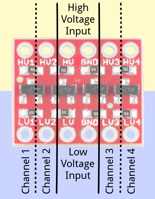
The Pinout:
The LC-04 logic level converter has two types of pins:
- Voltage input pins :
- 2 pins (GND and LV) on Low Voltage side
- 2 pins (GND and HV) on High Voltage side
- Data channels :
- 4 pins (LV1, LV2, LV3, and LV4) on Low Voltage side
- 4 pins (HV1, HV2, HV3, and HV4) on High Voltage side
Pin HV and LV set HIGH (logic 1) logic level on High voltage side and Low voltage side respectively, with respect to the GND.
Data channel pins shift logic levels from one voltage reference to another. A low voltage signal sent into LV1, for example, will be shifted up to the higher voltage and sent out through HV1. Similarly, a high voltage signal sent into HV1 will be shifted down to the lower voltage and sent out through LV1.
Read more: LC-04 4 Channel Logic Converter 3.3V – 5.0V
- How does the LC-04 handle signal direction?
The module shifts logic levels bi-directionally, stepping down 5V to 3.3V and stepping up 3.3V to 5V simultaneously. - What frequency signals can this converter process?
It converts high frequency signals such as 400KHz I²C, SPI, and UART without delay. - What are the voltage ranges for the LV and HV sides?
The Lower-voltage supply ranges from 1.5V to 7V, while the Higher-voltage supply ranges from LV to 18V. - How many data channels does the LC-04 support?
The module offers bi-directional shifting for up to four channels. - Does the module require external pull-up resistors?
No, the board includes 10K Ohm pull-up resistors connected to the respective power supplies. - Is the LC-04 suitable for breadboard use?
Yes, it features breadboard-compatible pin spacing and a small size of 0.4″ × 0.5″ × 0.08″. - What happens if a low voltage signal enters LV1?
A low voltage signal sent into LV1 will be shifted up to the higher voltage and sent out through HV1. - How do the GND pins function on the device?
GND pins on both sides establish the ground reference necessary for setting HIGH logic levels on their respective sides.
