Summary of 10 Million YouTube Subscribers Award LED PCB
This project is a Play Button–shaped LED PCB that cycles through five lighting modes (all off, silver, gold, sparkling diamond, and all red) using an ATTiny85 microcontroller, a button, and a switch. The 150mm x 100mm board is powered by a 3.7V drone battery (about 30 minutes at full brightness) and was developed for a Berry College class. Design and fabrication use EasyEDA, surface-mount assembly with solder paste, and programming via a custom programmer, USB programmer, or Arduino method.
Parts used in the 10 Million YouTube Subscribers Award LED PCB:
- Surface mounted ATTiny85 Microcontroller (C89852)
- USB Programmer
- ATTiny with IC sockets (ATTiny85-20PU THT)
- Button (C86487)
- Header pins for power connection (C86471)
- 10k Ohm resistor (C99198)
- RGB LEDs (C114585)
- 100 nF Capacitors (C1590)
- Switch (C128955)
- 4.7 uF Capacitor (C108344)
- Drone battery and charger
- Solder paste (MG Chemicals leaded solder paste)
Summary
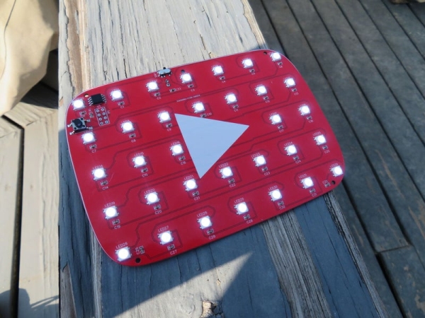
This PCB (Printed Circuit Board) resembles the YouTube Play Button award that is given out to creators for reaching certain milestones such as 100,000, 1 million, and 10 million subscribers. When the switch is turned on, the user can scroll through 5 different modes by pressing the button on the top left corner. The first mode leaves all the LED’s OFF, the second is silver (100,000 subs), the third is gold (1 million subs), the fourth is a sparkling diamond effect (10 million subs), and the fifth, just to match the board color, is all red. The board is about 150mm x 100mm, it has holes in the corners so it could be mounted somewhere, however, I have not mounted it to anything. The board is currently powered by a 3.7-volt drone battery, I might change this so that I can just leave it plugged in and mount it somewhere and not have to worry about changing the battery as it only lasts about 30 minutes with the LEDs at full brightness.
This board was built for a Special Topics Class at Berry College taught by Zane Cochran who had the idea of using images to design and inspire PCB builds.
Components
Unlike Slouchy Board and the Desktop Device that I built, I did not breadboard this circuit as it was just LED’s, a switch, a button, and an ATTiny85 microcontroller. All of the components that I used (all the surface mounted stuff), except for the batteries, can be found on https://lcsc.com/ for super cheap and are listed below.
We used a custom-built programmer (by Zane) to program the boards while they were already surface mounted on the board. Since those are not commercially available, you’d have to either build your own or use the ATTiny with mounted sockets and the USB programmer. Or you could program the ATTiny through an Arduino if you make the header pin holes large enough on the PCB for jumper wires (sort of as shown in the video linked at the end of this video).
Surface mounted ATTiny85 Microcontroller C89852 ($2 each)
($27) USB Programmer
($11) ATTiny + IC sockets
Button C86487 ($0.20 each)
Header pins for power connection C86471 ($0.20 each)
10k Ohm resistor C99198 ($.08 for 100)
RGB LED C114585 ($0.50 for 5, $3.70 for 50)
100 nF Capacitor C1590 ($0.29 for 50)
Switch C128955 ($0.41 for 5)
4.7uF Capacitor C108344 (20 for $0.37)
Drone battery and charger perfect for powering low voltage circuits($23)
Tools/Software
To create the PCB, you can go to EasyEDA and make a free account, You can reference my Slouchy Board or Desktop Device Instructables for help with EasyEDA as those both show how to use it. The PCB’s range from $5-$10 for 5 and take about a week or two to ship from China to the US.
Once you get your PCB from China and you have all your components ready, you will need to use Solder Paste to attach each individual component. I used MG Chemicals Leaded Solder Paste. (CAREFUL, THIS PRODUCT DOES HAVE LEAD IN IT. I think they also make some lead free solder paste)
To program, the ATTiny85, use Arduino’s Software but make sure that you have the board files downloaded if you have never programmed an ATTiny85. This video does a great job of explaining how to do that: Tutorial: Programming the Attiny 85 with an Arduino.
Step 1: EasyEDA: Schematic
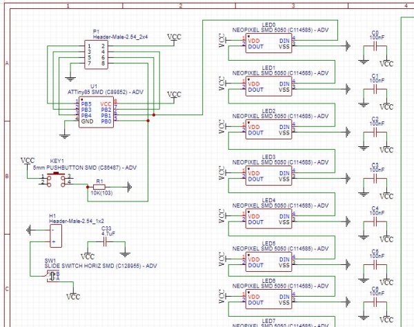
On EasyEDA, start by creating a new project and make a new schematic. Make sure you place the components that I list below and connect them similar to how I have it on the schematic. On the left side, you can search the various libraries for the parts required and then place them in the schematic.
For programming the Microcontroller while in the board, use a surface mounted ATTiny or a Through hole ATTIny.
Surface mounted ATTiny85 Microcontroller (Go to the “libraries” on the left and search “C89852”), to make the connections for jumper wires go to EELib on the left and chose a 2×4 male header pin as shown in the image. This means you could temporarily solder jumpers in place to program the board via an Arduino.
OR
Socket mounted ATTiny85 (Go to the “libraries” on the left and search “Attiny85-20PU THT” by AutogolazzoJr) this will place the footprint of the socket on the board which you can then solder in. This allows you to move the controller back and forth but means you have to have that USB controller which is quite pricey.
place all of the following
(1x on the back) Header pins for power connection (Go to the “libraries” on the left and search “C86471”)
(1x with button) 10k Ohm resistor (Go to the “libraries” on the left and search “C99198”)
(However many you want)RGB LED (Go to the “libraries” on the left and search “C114585”)
(One per LED)100 nF Capacitor (Go to the “libraries” on the left and search “C1590”)
(1x) Switch (Go to the “libraries” on the left and search “C128955”)
(1x) 4.7uF Capacitor (Go to the “libraries” on the left and search “C108344”) Place this capacitor near the power header pins but make sure it is on the front, you can only surface solder on one side. (Otherwise, things fall off when you heat up the board)
Once you have all the components placed, connect them to the correct pins as well as the GDN and VCC connections. You connect them by using the wiring tool and placing the GND & VCC symbols. Then once you have properly connected all the wires, you can click the convert to PCB button.
Step 2: EasyEDA: PCB Design
Before you get to the PCB environment use Inkscape or some other software that you can use to create DXF files and make an outline of your chosen shape. Once you have a DXF file of your shapes outline that has been sized to the correct units (150mmx100mm for example) create a separate file that contains what will be drawn on the board, for me it was just the triangle of the play button.
When you start in the PCB environment, you’ll see a bunch of layers and numbers on the right. Change your units to millimeters or whatever you want to use and change the snap size (snap size is basically at what interval you can place things on the grid) to something convenient. I made mine 10mm since I wanted my board outline to be easily placed at (0, 0).
Start by editing the board outline layer (click the color and a pencil should appear) and import the outline DXF file. Once you have this, edit your top layer and start placing the components on the board how you want them by dragging them onto the outline. Then once the components are placed, connect all blue lines with the wire tool, unless they are connected to GND or VCC. The GND and VCC connections connect directly to the board and don’t need to be isolated via the wires.
Once all non-VCC and GND connections are wired together, you can use the Copper area tool to make the last connections. Do this once on the top layer and once on the bottom layer. Make sure that you change one of the copper areas to VCC in the properties tab, I usually make the top layer GND and the bottom layer VCC. Once you have that done, the board should look complete and you can zoom in to see where GND connects to the board. At this point, you want to check for DRC Errors by refreshing the DRC Errors under the Design Manager tab on the far left. If there are no errors, you are good to go and order your board.
One last important thing you need to do if you are going the jumper wire route with Surface Mounted ATTiny is editing the holes of the header pin connections. Click on the 2×4 header pin connection, go to the right under properties and change the hole (Diameter) to 1mm. I think this should do if you solder the wires in place, make sure you do this for each hole.
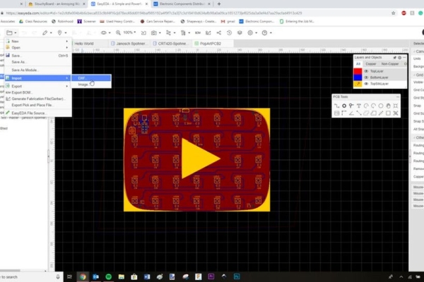
To order your board, click the button in the top ribbon with a G and right facing arrow to export your Gerber file. This will take you directly to where you purchase your boards, there are lots of options for different colors and finishes which will affect the price of the board, for PCB thickness, I think 1.6 is what we usually do. If you want to double check that your components fit, you can export a PNG image of your board and then push your components through the paper to see that the prongs all fit. Don’t worry about scaling it, you should be able to just print it out.
(Edit) I have added the Gerber file if you would like to use it.
Read more: 10 Million YouTube Subscribers Award LED PCB
- What does the PCB look like and what is its size?
The PCB resembles a YouTube Play Button award and measures about 150mm x 100mm. - How many lighting modes does the board have and what are they?
It has five modes: all LEDs off, silver (100,000 subs), gold (1 million subs), sparkling diamond (10 million subs), and all red. - What powers the board and how long does it last?
The board is powered by a 3.7-volt drone battery and lasts about 30 minutes at full LED brightness. - Which microcontroller is used to control the LEDs?
The project uses an ATTiny85 microcontroller. - How are the components assembled on the PCB?
Components are surface mounted using solder paste; the ATTiny85 can be surface mounted or socket mounted for programming. - How can the ATTiny85 be programmed?
It was programmed using a custom programmer; alternatively use a USB programmer, Arduino, or socket with a USB programmer. - What software and service are recommended for PCB design and ordering?
EasyEDA is recommended for design and exporting Gerber files, and PCBs can be ordered from China via EasyEDA for about $5–$10 for five boards. - What precautions are mentioned for solder paste?
MG Chemicals leaded solder paste was used and it contains lead, so take care; there may be lead-free alternatives.