
Summary of NXP ANNOUNCES GENERAL AVAILABILITY OF THE ARM CORTEX-M33-BASED LPC551X S1X MCU FAMILY
NXP announced the LPC551x/S1x MCU family, expanding the LPC5500 series with power-efficient, secure Arm Cortex-M33 devices using 40-nm flash. Key benefits include low power (as low as 32 µA/MHz), over 600 CoreMarks, up to 150 MHz core, up to 256 KB flash and 96 KB SRAM, CAN FD, dual-USB with on-chip PHY, SDIO and up to 9 FlexComm interfaces, and hardware security features (SRAM PUF root key, secure boot, TrustZone, PRINCE cipher, crypto accelerators, authenticated debug). Available in HLQFP100, VFBGA98, and HTQFP64, supported by MCUXpresso.
Parts used in the LPC551x/S1x MCU family:
- Arm Cortex-M33 core (up to 150 MHz)
- On-chip flash memory (up to 256 KB)
- On-chip SRAM (up to 96 KB)
- 40-nm flash process technology
- CAN FD / CAN 2.0 interface
- Dual-USB with on-chip PHY (HS and FS modes)
- SDIO interface
- FlexComm interfaces (up to 9, configurable as SPI/I2C/I2S/UART)
- SRAM PUF based device root key hardware
- Secure boot and anti-rollback protection mechanisms
- Arm TrustZone technology for resource isolation
- PRINCE hardware block cipher for internal flash encryption/decryption
- Cryptographic accelerators for symmetric and asymmetric algorithms
- Authenticated debug capability
- Package options: HLQFP100, VFBGA98, HTQFP64
- MCUXpresso software and tools support
NXP Semiconductors today announced the availability of its LPC551x/S1x microcontroller (MCU) family – further extending its performance-efficient LPC5500 MCU series. The LPC551x/S1x MCU family offers developers low power consumption, embedded security, pin-, software- and peripheral-compatibility to accelerate time-to-market. The LPC551x/S1x family leverages ultra-efficient 40-nm flash technology for cost and performance benefits.
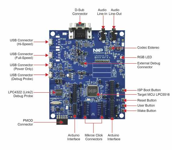
Key features include:
- Over 600 EEMBC® CoreMarks® and as low as 32uA/MHz
- Up to 150 MHz Arm® Cortex®-M33 core
- Up to 256 KB on-chip flash; up to 96 KB SRAM
- CAN FD / CAN 2.0 with MCUXpresso-based software enablement
- Dual-USB with on-chip PHY, supporting both HS and FS modes
- SDIO and up to 9 FlexComm interfaces (configurable as either SPI/I2C/I2S,UART)
- Advanced security enabled with MCUXpresso software and tools:
- SRAM PUF based device root key with added application key storage options
- Secure boot and anti-rollback protection
- Arm TrustZone® technology for resource isolation
- Hardware block cipher (PRINCE) for encryption/decryption of internal flash
- Accelerators for symmetric and asymmetric cryptography
- Authenticated debug capabilities
- Available in HLQFP100, VFBGA98 and HTQFP64 packages
- LPC551x/S1x is fully supported by NXP’s MCUXpresso suite of software and tools
To learn more about the LPC551x/S1x MCU family, please visit: www.nxp.com/LPC551x.
Read more: NXP ANNOUNCES GENERAL AVAILABILITY OF THE ARM CORTEX-M33-BASED LPC551X S1X MCU FAMILY
- What core does the LPC551x/S1x use?
It uses an Arm Cortex-M33 core running up to 150 MHz. - How much on-chip flash and SRAM are available?
The family offers up to 256 KB on-chip flash and up to 96 KB SRAM. - Does the MCU support CAN interfaces?
Yes, it supports CAN FD and CAN 2.0 with MCUXpresso-based software enablement. - Can the LPC551x/S1x handle USB connectivity?
Yes, it has dual-USB with on-chip PHY supporting both high-speed and full-speed modes. - How many FlexComm interfaces are available and what can they be configured as?
Up to 9 FlexComm interfaces configurable as SPI, I2C, I2S, or UART. - What security features are included?
Security features include SRAM PUF root key, secure boot and anti-rollback, Arm TrustZone, PRINCE block cipher, crypto accelerators, and authenticated debug. - What process technology do these MCUs use?
They leverage ultra-efficient 40-nm flash technology. - Which package options are available for LPC551x/S1x?
Available packages are HLQFP100, VFBGA98, and HTQFP64. - Is there software support for development?
Yes, the family is fully supported by NXP’s MCUXpresso suite of software and tools. - How energy efficient is the MCU?
Performance includes as low as 32 uA per MHz and over 600 EEMBC CoreMarks.
