
Summary of Making the Electronics for CDM324 – 24GHz Doppler Motion Sensor
The article examines the CDM324 24.125 GHz Doppler motion sensor (likely a clone of InnoSenT IPM165), compares it to HB100, and documents designing a proper amplification and comparator circuit. It critiques common Chinese amplifier boards, presents a chosen two-stage op-amp design using OPA2365 for stable gain and bandwidth, shows final schematics, PCB and 3D holder, and provides Arduino and Python sample code to measure and display detected speed.
Parts used in the CDM324 Doppler Motion Sensor Project:
- CDM324 24.125 GHz Doppler motion sensor module
- OPA2365 operational amplifier (dual op-amp)
- LM258 (mentioned in critique of poor designs)
- Comparator IC (U2 in schematics)
- Various resistors (for gains of 125.5 per stage and biasing)
- Various capacitors (for bandpass filtering and decoupling, including C10)
- Ferrite bead FB1 (power supply filtering)
- Transistor Q1 (for pulse mode using nEN pin)
- 3-pin header (connection to sensor)
- 0805 SMD passive components (resistors and capacitors)
- PCB (25x25 mm assembled board)
- 3D printed holder/enclosure
The Doppler Effect
I’m sure you’re quite familiar with the Doppler effect: you send an RF signal at a given frequency to a target, and if this object/person is moving the reflected signal’s frequency will be shifted. This is the reason why a fire truck’s siren has a higher pitch when the truck is going towards you than when it is going away.
The CDM324 / IPM165 Motion Sensor
You may recall the article I wrote a couple of years ago about a nearly identical Doppler sensor, the HB100.
While the HB100 is using a 10.525GHz frequency, this new module uses 24.125GHz! This has the main advantage of being compatible with European regulations (ETSI #300 400) and having good penetration in dry materials. Moreover, as the main frequency is higher the patch antennas are smaller, hence the tiny 25x25x6mm module.
This motion sensor can easily be purchased on eBay under the name CDM324. Oddly enough, looking for “cdm324” on your favorite search engine won’t bring any interesting results.
I therefore spent several hours tracing the origins of this tiny sensor. I finally arrived to the conclusion that it likely is a clone of the InnoSenT IPM 165, which is itself very similar to the AP96 from Agilsense.
Specification-wise, the CDM324 antenna pattern is slightly narrower than the HB100’s: 80° azimuth and 32° elevation versus 80° azimuth and 40° elevation. The Radiated Power (EIRP) is more or less the same: 16dBm vs 15dBm. Finally, the advertised power consumption is identical to the HB100’s: up to 40mA @ 5V.
Finding the Right Amplification Circuit
Now that I had traced the origins of this CDM324, I could find its recommended amplifier schematics.
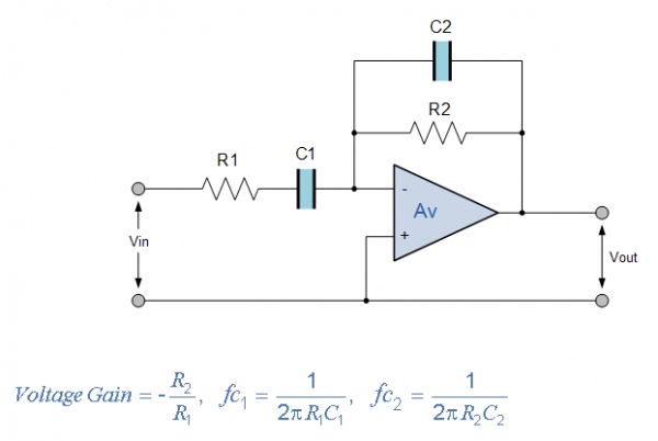
The one you see above comes from InnoSenT. It consists in 2 cascaded inverting band pass filter circuits:
You’ll however notice that the op-amp positive input in our suggested schematics is tied to vcc/2, allowing us to have a centered amplification output as well.
From the formulas above, we can compute the circuit total gain and cutoff frequencies. I’ll spare you the maths, the suggested amplification is 1018 (60dB) and a band pass filter from 3.4Hz to 1.06kHz.
The InnoSenT application note allows us to put these frequencies in context:
The high cutoff frequency is therefore set for a 24km/h or 15.4m/h speed. However, this isn’t exactly true as the filter cutoff slope isn’t vertical. Here’s the simulated amplification output generated using LTspice:
You may therefore be able to measure much higher speeds if the moving object is close to the sensor.
Amplification Circuit from Chinese Sellers
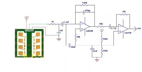
This is the (very low resolution) recommended amplification circuit that you will find online.
Simulating it leads to raising eyebrows:
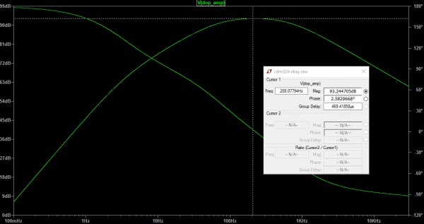
Many many things are odd with this recommended amplification circuit:
– No high pass filter on the second amplifier (remember, the cutoff slope in the first amplifier stage isn’t vertical)
– I don’t see any reason for that 1nF capacitor when the high pass filter is done using the first op-amp
– Amplification on the first stage is 510 while the amplification on the second stage is 100
– Which leads to a total gain of 51000 (94dB)
– … while the LM258 has a gain bandwidth product of 1MHz!
The last point is crucial. Given the first amplification stage has a gain of 510, this means there’s only 1.96kHz of bandwith “left” inside the LM258. As the cutoff slope isn’t vertical, this means that the LM258 isn’t the right op-amp for the job! For example, at 10kHz the amplification is 3162, which is a GBW product of 31.6MHz!
Chosen Amplification Circuit:
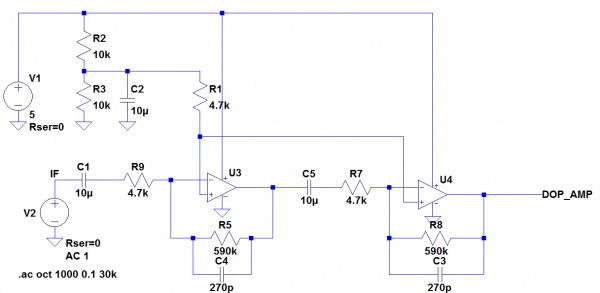
After lots of experimentation and performance comparisons with my previous HB100 module, you can see above the final amplification circuit I chose.
– As you can imagine, it is based on the manufacturer’s
– Each amplification stage has a gain of 125.5
– Total gain is therefore 15758 (84dB)
– Cutoff frequencies are 3.4Hz and 999Hz (< 1 km/h or m/h and 22.7km/h / 14.5m/h respectively)
Not so surprisingly the total gain is quite close to the one I had set on the HB100 (12100) and I’m fairly sure I could have set the same one. It was simply more convenient to choose the same resistors & capacitors values in my circuit.
As with my previous HB100 amplification circuit, I chose the OPA2365 operational amplifier. It has a 50MHz Gain Bandwidth product, which is more than the 15758*(84dB-3dB) = 11.2MHz product at the high cutoff frequency point.
Final Schematics
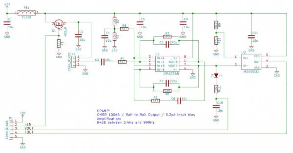
You can see above the final schematics:
– FB1 is here to filter the power supply noise
– the voltage at the C10/R11 node is proportional to the amount of reflected RF energy
– Q1 allows pulse mode operation: you may power on/off the CDM324 using the module nEN pin
– U2 is a simple comparator that will transform our amplified output to a neat square wave:
In the scope capture above the yellow trace is the amplified output while the pink one is the comparator’s output.
Using a comparator is a simple way to ‘extract’ the amplified output main frequency but I’m quite sure running an FFT on that signal would be quite interesting!
Assembled PCB
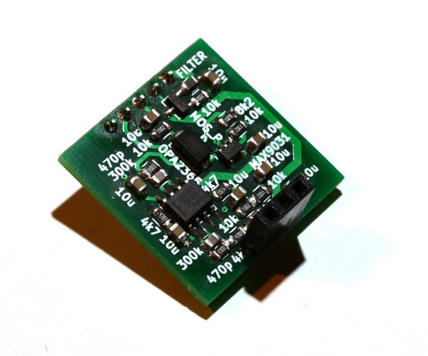
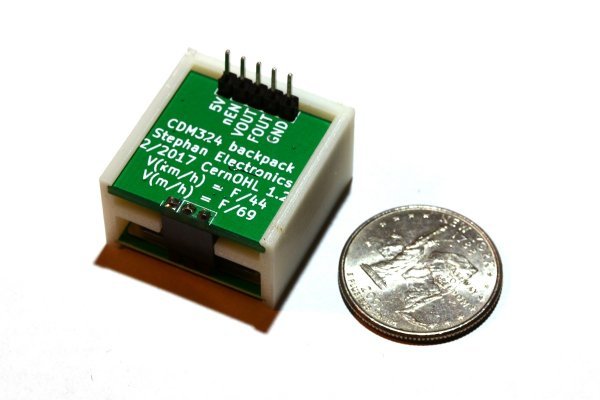
Here’s what the assembled PCB looks like! It has the same size as the CDM324 (25x25mm) and uses a 3pins header to connect with the sensor. 0805 passive components were chosen to make the soldering job easier.
Please do not pay attention to the silkscreen as some values have changed since then: have a look at the end of this article to download all the source files.
3D Printed Holder
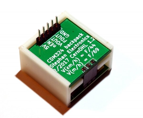
The HB100 doppler module had 4 connectors at each corner to solder my ‘backpack PCB’ to.
Unfortunately the CDM324 only offers a single 3 pins connection, which is why I designed and 3D printed a neat assembly holder: the CDM324 with its amplification circuit simply slide in it!
The Sensors in Action & Sample Code
Here’s the video of the HB100 and CDM324 working side by side!
I’m guessing that if you were to use such a module you’d definitely like some sample code.
Below is some arduino code that will output the detected speed in your favorite terminal:
// Below: pin number for FOUT #define PIN_NUMBER 4 // Below: number of samples for averaging #define AVERAGE 4 // Below: define to use serial output with python script //#define PYTHON_OUTPUT unsigned int doppler_div = 44; unsigned int samples[AVERAGE]; unsigned int x; void setup() { Serial.begin(115200); pinMode(PIN_NUMBER, INPUT); } void loop() { noInterrupts(); pulseIn(PIN_NUMBER, HIGH); unsigned int pulse_length = 0; for (x = 0; x < AVERAGE; x++) { pulse_length = pulseIn(PIN_NUMBER, HIGH); pulse_length += pulseIn(PIN_NUMBER, LOW); samples[x] = pulse_length; } interrupts(); // Check for consistency bool samples_ok = true; unsigned int nbPulsesTime = samples[0]; for (x = 1; x < AVERAGE; x++) { nbPulsesTime += samples[x]; if ((samples[x] > samples[0] * 2) || (samples[x] < samples[0] / 2)) { samples_ok = false; } } if (samples_ok) { unsigned int Ttime = nbPulsesTime / AVERAGE; unsigned int Freq = 1000000 / Ttime; #ifdef PYTHON_OUTPUT Serial.write(Freq/doppler_div); #else //Serial.print(Ttime); Serial.print(“\r\n”); Serial.print(Freq); Serial.print(“Hz : “); Serial.print(Freq/doppler_div); Serial.print(“km/h\r\n”); #endif } else { #ifndef PYTHON_OUTPUT Serial.print(“.”); #endif } }
Text written in serial terminals is so small though… why not print it bigger using ASCII art?
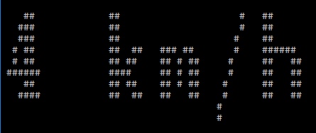
Simply define PYTHON_OUTPUT in the script above, install python on your computer, run “pip install pyfiglet pyserial” and use that awesome little python script (don’t forget to replace COM3 with your COM port):
from pyfiglet import *
import serial
import os

ser = serial.Serial('COM3', 115200)
while True:
	speed = ord(ser.read())
	os.system('cls||clear')
	print(figlet_format(" ",font="clb8x10"))
	print(figlet_format(" ",font="clb8x10"))
	print(figlet_format(str(speed)+" km/h",font="clb8x10"))
	print(figlet_format(" ",font="clb8x10"))
Source: Making the Electronics for CDM324 – 24GHz Doppler Motion Sensor
- What is the main frequency of the CDM324 module?
The CDM324 uses a 24.125 GHz center frequency. - How does the CDM324 compare to the HB100 in antenna pattern?
CDM324 has about 80° azimuth and 32° elevation versus HB100's 80° azimuth and 40° elevation. - What total gain and cutoff frequencies were chosen for the amplification circuit?
Total gain is 15758 (84 dB) with cutoff frequencies 3.4 Hz and 999 Hz. - Why was the OPA2365 op-amp chosen?
Because it has a 50 MHz gain-bandwidth product sufficient for the designed total gain and bandwidth requirements. - What problem was identified with many Chinese seller amplifier circuits?
Their designs had excessively high total gain (about 51000), missing high-pass on the second stage, odd capacitor placement, and used LM258 whose GBW was inadequate for that gain. - How is the amplified output converted to a usable signal?
A comparator (U2) transforms the amplified analog output into a square wave signal. - What is the purpose of FB1 on the final schematic?
FB1 filters power supply noise. - How is pulse mode operation implemented?
Q1 allows powering the CDM324 on/off using the module nEN pin for pulse mode. - Is sample code provided for reading detected speed?
Yes, Arduino code is provided to measure frequency and convert to km/h, plus an optional Python script to display large ASCII output. - What physical form factor was used for the amplification PCB?
The PCB matches the CDM324 size (25x25 mm) and uses 0805 passive components and a 3-pin header.
