 The dominant technology for today’s high-brightness LEDs is gallium nitride (GaN) on sapphire, silicon carbide (SiC), or silicon-substrate LEDs. These materials are popular because the resultant LEDs are bright, efficient, and last a long time. However, the chips are tough to manufacture and package into useable devices, multiplying the cost of end products that use them as light engines. Although prices have plummeted in recent years, LED lighting is still considerably more expensive to purchase than traditional alternatives. This initial expense is cited as a major factor slowing the acceptance of solid-state lighting (SSL).
A pioneering group of manufacturers has worked hard to reduce the cost of high-power LEDs by replacing the sapphire or SiC substrate with silicon (Si), the material routinely used to manufacture most electronic chips (“ICs”). The key benefit is a very-low-cost supply of wafers and the opportunity to use depreciated 8-inch wafer fabs for LED manufacture. Combined, those concepts enable a dramatic reduction in LED prices, overcoming consumer objections.
Initially, technical challenges limited the performance of GaN-on-Si LEDs, making them unattractive for mainstream lighting. Now, some manufacturers, notably Toshiba, have introduced a new generation of these LEDs with vastly improved performance at a very competitive price, making them a viable alternative to conventional devices in many applications.
This article reviews the development of silicon-substrate LEDs and describes the latest generation of commercial devices.
Pushing down the cost of LEDs
Though it’s taken many years and millions of dollars of R&D funding, modern LEDs are a cost-effective alternative to traditional light sources such as incandescent bulbs, fluorescent tubes, and halogen lamps for mainstream lighting when factors such as initial purchase price, energy consumption, and lifetime are taken into consideration to determine “cost of ownership.”
A recent report1 by analysts McKinsey & Company concluded that by 2016 (depending on how quickly the price of LEDs continues to fall) the payback on an LED fixture (due to lower running costs and longer life) will offset the initial higher purchase price compared to a compact fluorescent lamp (CFL) between 1.7 and 3.9 years. The corresponding calculation in 2011 yielded a figure of around 14 years. Payback time of LED bulb vs. CFL bulb in the residential segment (dark line represents base case, lighter line represents faster LED price erosion). (Courtesy of McKinsey & Company)
Unfortunately, the same report concluded that, despite the market share of LEDs in lighting applications climbing to around 45 percent in 2015, “the price premium on LED lighting products still remains high, and the initial purchase price represents a significant barrier to decision makers when considering an initial investment in general lighting applications.”
This reticence is perhaps not surprising when considering that an LED lamp replacement such as Philips’ 100 W (incandescent) equivalent PAR38 LED bulb retails at $22 compared with $12 for the same company’s 100 W equivalent T2 Twister CFL and $6 for a 100 W equivalent EcoSmart halogen bulb.
A key element of the cost of LED bulbs is the LED chips themselves. Each LED bulb typically comprises an array of six, eight, or ten LED chips, each of which is manufactured from exotic materials in a complex wafer-fabrication process and then expensively packaged in a three- or four-step assembly operation. Replacing both the material and manufacturing costs with cheaper alternatives would dramatically reduce the initial purchase price of LEDs, encouraging more rapid adoption.
The silicon alternative
The electronics revolution has been built on silicon; a stable, cheap, plentiful semiconductor that’s easy to grow into crystals, slice into wafers, and subject to CMOS processes to turn each wafer into thousands of ICs. In addition, a huge investment has been made in fabs to mass-produce such chips, driving down the cost per unit to mere cents.
Recently, chip manufacturers have moved to a more efficient wafer-fabrication process that uses 12-inch (300 mm) wafers as raw material, replacing the older 8-inch (200 mm) slices. As a result, there is an excess of 8-inch capacity around the world which some suggest could be turned to LED manufacturing, dramatically cutting the price of the end products.
The majority of contemporary LEDs are constructed from a combination of GaN, which features a band gap suitable for emitting photons in the visible part of the spectrum, on a sapphire substrate. GaN thin films are grown by a process known as epitaxy, which builds up the LED’s active regions by depositing successive layers on the substrate. One drawback is a mismatch between the crystal lattice spacing (the unit distance between individual atoms in the crystal structure) of GaN and the sapphire substrate which results in microscopic flaws in the active region. These flaws, also known as threading dislocations, compromise both LED luminosity and lifetime.
SiC has a crystal structure that is much more closely matched to GaN than sapphire, reducing the defect density, and improving efficacy and longevity by at least one and sometimes two orders of magnitude. (See the TechZone article “Material and Manufacturing Improvements Enhance LED Efficiency.”)
Sapphire and SiC are not only expensive to produce but are also difficult to reliably manufacture on wafers larger than 4 inches (100 mm) in diameter. Besides being much cheaper and easier to work with, 8-inch silicon wafers take only slightly longer to process than wafers measuring 4 inches. The end result is that factories can quadruple production (the surface area of an 8-inch wafer is four times that of a 4-inch one (Figure 2), while at the same time slashing material and processing costs.
However, switching to silicon as a substrate for LEDs presents formidable technical challenges. Chief among these is the fact that silicon’s crystal structure is an even worse mismatch with GaN than sapphire. To make matters worse, silicon has a very different coefficient of thermal expansion to GaN. These two factors lead to severe tensile stresses being incorporated into the wafers during fabrication that result in microcracking as the wafer cools. Cracked LEDs function poorly, if at all. Worse yet, silicon is a very good absorber of the photons that should escape and contribute to the luminosity of the LED. As a result, light extraction from early GaN-on-Si LEDs was a quarter to a third of that from comparable devices built on sapphire (see the TechZone article “Will Silicon Substrates Push LED Lighting Into the Mainstream?”)
A few pioneering companies have persevered with their development programs, and while GaN-on-Si LEDs still lag the luminosity, efficacy, and long life of GaN-on-sapphire or on-SiC LEDs, the devices on today’s lab benches don’t suffer from the poor performance of earlier devices and can be made at a fraction of the cost of conventional LEDs.
Second-generation silicon
As conventional LEDs have steadily improved (at the same time reducing the number of LEDs required to match the output of single incandescent or fluorescent bulbs) a new market opened up for “mid-range” LEDs. Mid-range chips cannot match the performance of today’s high-end devices, but instead offer reasonable performance (for example, providing luminosity and longevity equivalent to the top spec chip of two or three years ago) at a budget price (see the TechZone article “Mid-Power LEDs Offer Less Expensive Alternative for Lighting Applications”).
The growth of the mid-range market has opened up an opportunity for GaN-on-Si chips. The performance of today’s silicon-substrate LEDs can easily match that of mid-range GaN-on-sapphire or on-SiC while undercutting the latter’s price.
Toshiba (which originally worked in a joint venture with Bridgelux but later bought out its partner’s share in the venture) is one of the commercial frontrunners in the supply of GaN-on-Si LEDs.
Toshiba is understandably coy about how it has solved the technical difficulties of lattice- and thermal- mismatch between GaN and Si and has made few public pronouncements, but before being bought out, Bridgelux did reveal that the “tensile strain problem was solved using a proprietary buffer layer (between the GaN and the silicon).”
Further information about Toshiba’s research is available in scientific papers. One example2 published in February 2006 describes how Toshiba researchers suppressed the crack generation that typically plagues GaN epitaxy on silicon by employing “cubic SiC” as intermediate layers. Cubic SiC has a lattice constant about half way between GaN and silicon, helping to relieve the stresses that would otherwise build up and cause cracking between abutted layers of GaN and silicon.
The researchers reported that a 1 µm layer of SiC on top of a conventional 8-inch silicon wafer was sufficient to suppress cracking in the active GaN layer. While slightly more expensive than depositing GaN onto “naked” silicon, the process is still much less expensive than fabricating sapphire or SiC wafers because it is still founded on the inexpensive silicon manufacturing processes.
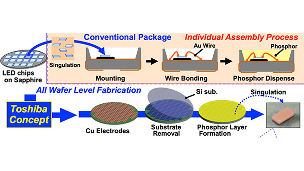
Toshiba also claims its GaN-on-Si process lends itself to the production of large “volume-emitting” single-LED chips directly from the wafer without the need to go through the traditional LED assembly process (Figure 3). The advantages of this technique are greater cost savings and single LEDs which could compete with increasingly popular Chip-on-Board (CoB) arrays – products that comprise multiple conventional LEDs pre-assembled into a single unit (see the TechZone article “The Rise of Chip-on-Board LED Modules”).
For more detail: Improved Silicon-Substrate LEDs Address High Solid-State Lighting Costs