Summary of Girino – Fast Arduino Oscilloscope using Arduino power connector
This article details the construction of "Girino," a high-speed homebrew Arduino oscilloscope designed to overcome the latency of standard serial-based projects. The author utilizes direct register manipulation, hardware triggers via the Analog Comparator, and a circular buffer for continuous data acquisition to maximize velocity on the ATMega328P microcontroller.
Parts used in the Girino:
- Arduino board
- ATMega328P microcontroller datasheet
- Analog Comparator
- Circular buffer (array of 1280 slots)
- Signal decoupling circuitry
- Signal offset circuitry
- Hardware trigger mechanism
I am a Physicist and the nicest part of working in this field is that I get to build my own instruments. With this way of thinking, I decided to build a homebrew Arduino Oscilloscope. This instructable was written with the purpose of teaching a bit about microcontrollers and data acquisition. This is an extreme project because I wanted to squeeze out from Arduino as much velocity as I could, I have not seen any other Arduino Oscilloscope as fast as this one.
Some time ago I was working on an Arduino project and I needed to see if the output signal was into compliance with the specifics. Thus I spent some time on the internet looking for Arduino Oscilloscopes already implemented, but I did not like what I found. The projects that I found were mostly composed of a Graphical User Interface for the computer written in Processing and a very simple arduino sketch. The sketches were something like:
void setup() {
Serial.begin(9600);
}void loop() {
int val = analogRead(ANALOG_IN);
Serial.println(val);
}
This approach is not wrong and I do not want to insult anyone, but this is too slow for me. The serial port is slow and sending every result of an analogRead() through it is a bottleneck.
I have been studying Waveform Digitizers for some time and I know reasonably well how do they work, so I got inspiration from them. These were the starting points of the oscilloscope that I wanted to create:
- the incoming signal should be decoupled from the arduino to preserve it;
- with an offset of the signal it is possible to see negative signals;
- the data should be buffered;
- a hardware trigger is required to catch the signals;
- a circular buffer can give the signal shape prior to the trigger (more to follow on this point);
- using lower lever functions that the standard ones makes the program run faster.
The sketch for the Arduino is attached to this step, along with the schematic of the circuit that I made.
The name that I came up with, Girino, is a frivolous pun in Italian. Giro means rotation and adding the suffix -ino you get a small rotation, but Girino also means tadpole. This way I got a name and a mascot.
Step 2: What you need
What we really need for this project is an Arduino board and the datasheet of the ATMega328P.
The datasheet is what tells us how the microcontroller works and it is very important to keep it if we want a lower lever of control.
The datasheet can be found here: http://www.atmel.com/Images/doc8271.pdf
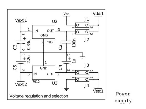
The hardware that I added to the Arduino is partly necessary, its purpose is just to form the signal for the ADC and to provide a voltage level for the trigger. If you want, you could send the signal directly to the Arduino and use some voltage reference defined by a voltage divider, or even the 3.3 V given by the Arduino itself.
Step 3: Debug output
I usually put a lot of debug output in my programs because I want to keep track of anything that happens; the problem with Arduino is that we do not have a stdout to write to. I decided to use the Serial port as a stdout.
Be aware, though, that this approach does not work all the times! Because writing to the Serial port requires some time for the execution and it can dramatically change things during some time sensible routines.
I usually define debugging outputs inside a preprocessor macro, so when the debug is disabled they simply disappear from the program and do not slow down the execution:
- dprint(x); – Writes to the serial port something like: # x: 123
- dshow(“Some string”); – Writes the string
Step 4: Setting register bits
With the purpose of being fast, it is necessary to manipulate the microcontroller features with lower lever functions than the standard ones provided by the Arduino IDE. The internal functions are managed through some registers, that are collections of eight bits where each one governs something particular. Each register contains eight bits because the ATMega328P has an 8-bit architecture.
The registers have some names that are specified in the datasheet depending on their meanings, like ADCSRA for the ADC Setting Register A. Also each meaningful bit of the registers has a name, like ADEN for the ADC Enable Bit in the ADCSRA register.
To set their bits we could use the usual C syntax for binary algebra, but I found on the internet a couple of macros that are very nice and clean:
// Defines for setting and clearing register bits
#ifndef cbi
#define cbi(sfr, bit) (_SFR_BYTE(sfr) &= ~_BV(bit))
#endif
#ifndef sbi
#define sbi(sfr, bit) (_SFR_BYTE(sfr) |= _BV(bit))
#endif
Using them is very simple, if we want to set to 1 the Enable Bit of the ADC we can just write:
sbi(ADCSRA,ADEN);
While if we want to set it to 0 (id est clear it) we can just write:
cbi(ADCSRA,ADEN);
Step 5: What are the Interrupts
The functions that are executed are called Interrupt Service Routines (ISR) and are more or less simple functions, but that do not take arguments.
Let us see an example, something like counting some pulses. The ATMega328P has an Analog Comparator that has an interrupt associated that is activated when a signal surpasses a reference voltage. First of all you must define the function that will be exectuted:
ISR(ANALOG_COMP_vect)
{
counter++;
}This is really simple, the instruction ISR() is a macro that tells the compiler that the following function is an Interrupt Service Routine. While ANALOG_COMP_vect is called Interrupt Vector and it tells the compiler which interrupt is associated to that routine. In this case it is the Analog Comparator Interrupt. So everytime that the comparator sees a signal bigger than a reference it tells the microcontroller to execute that code, id est in this case to increment that variable.
The next step is to enable the interrupt associated. To enable it we must set the ACIE (Analog Comparator Interrupt Enable) bit of the ACSR (Analog Comparator Setting Register) register:
sbi(ACSR,ACIE);
In the following site we can see the list of all Interrupt Vectors:
http://www.nongnu.org/avr-libc/user-manual/group__avr__interrupts.htmlStep 6: Continuously acquire with a circular buffer
I prepared some diagrams to make myself clear. The following points are referring to the images.
- On the first image we can see what I mean with continuous acquisition. We define a buffer that will store the data, in my case an array with 1280 slots, then we start to continuously read the ADC output register (ADCH) ad filling the buffer with the data. When we get to the end of the buffer we restart from the beggining without clearing it. If we immagine the array arranged in a circular way it is easy to see what I mean.
- When the signal surpasses the threshold, the Analog Comparator Interrupt is activated. Then we start a waiting phase in which we continue to acquire the signal but keep a count of the ADC cycles that passed from the Analog Comparator Interrupt.
- When we waited for N cycles (with N < 1280), we freeze the situation and stop the ADC cycles. So we end up with a buffer filled with the digitization of the signal temporal shape. The great part of this, is that we have also the shape prior to the trigger event, because we were already acquiring before that.
- Now we can send the whole buffer to the serial port in a block of binary data, instead of sending the single ADC reads. This reduced the overhead required to send the data and the bottleneck of the sketches that I found on the internet.
Step 10: Setting up the ADC
In the sketch, I wrote a initialization function that sets-up all the parameters of the ADC functioning. As I tend to write clean and commented code, I will just past the function here. We can refer to the preceding step and to the comments for the meaning of the registers. void initADC(void)
{
//———————————————————————
// ADMUX settings
//———————————————————————
// These bits select the voltage reference for the ADC. If these bits
// are changed during a conversion, the change will not go in effect
// until this conversion is complete (ADIF in ADCSRA is set). The
// internal voltage reference options may not be used if an external
// reference voltage is being applied to the AREF pin.
// REFS1 REFS0 Voltage reference
// 0 0 AREF, Internal Vref turned off
// 0 1 AVCC with external capacitor at AREF pin
// 1 0 Reserved
// 1 1 Internal 1.1V Voltage Reference with external
// capacitor at AREF pin
cbi(ADMUX,REFS1);
sbi(ADMUX,REFS0);
// The ADLAR bit affects the presentation of the ADC conversion result
// in the ADC Data Register. Write one to ADLAR to left adjust the
// result. Otherwise, the result is right adjusted. Changing the ADLAR
// bit will affect the ADC Data Register immediately, regardless of any
// ongoing conversions.
sbi(ADMUX,ADLAR);
// The value of these bits selects which analog inputs are connected to
// the ADC. If these bits are changed during a conversion, the change
// will not go in effect until this conversion is complete (ADIF in
// ADCSRA is set).
ADMUX |= ( ADCPIN & 0x07 );//———————————————————————
// ADCSRA settings
//———————————————————————
// Writing this bit to one enables the ADC. By writing it to zero, the
// ADC is turned off. Turning the ADC off while a conversion is in
// progress, will terminate this conversion.
cbi(ADCSRA,ADEN);
// In Single Conversion mode, write this bit to one to start each
// conversion. In Free Running mode, write this bit to one to start the
// first conversion. The first conversion after ADSC has been written
// after the ADC has been enabled, or if ADSC is written at the same
// time as the ADC is enabled, will take 25 ADC clock cycles instead of
// the normal 13. This first conversion performs initialization of the
// ADC. ADSC will read as one as long as a conversion is in progress.
// When the conversion is complete, it returns to zero. Writing zero to
// this bit has no effect.
cbi(ADCSRA,ADSC);
// When this bit is written to one, Auto Triggering of the ADC is
// enabled. The ADC will start a conversion on a positive edge of the
// selected trigger signal. The trigger source is selected by setting
// the ADC Trigger Select bits, ADTS in ADCSRB.
sbi(ADCSRA,ADATE);
// When this bit is written to one and the I-bit in SREG is set, the
// ADC Conversion Complete Interrupt is activated.
sbi(ADCSRA,ADIE);
// These bits determine the division factor between the system clock
// frequency and the input clock to the ADC.
// ADPS2 ADPS1 ADPS0 Division Factor
// 0 0 0 2
// 0 0 1 2
// 0 1 0 4
// 0 1 1 8
// 1 0 0 16
// 1 0 1 32
// 1 1 0 64
// 1 1 1 128
sbi(ADCSRA,ADPS2);
sbi(ADCSRA,ADPS1);
sbi(ADCSRA,ADPS0);//———————————————————————
// ADCSRB settings
//———————————————————————
// When this bit is written logic one and the ADC is switched off
// (ADEN in ADCSRA is zero), the ADC multiplexer selects the negative
// input to the Analog Comparator. When this bit is written logic zero,
// AIN1 is applied to the negative input of the Analog Comparator.
cbi(ADCSRB,ACME);
// If ADATE in ADCSRA is written to one, the value of these bits
// selects which source will trigger an ADC conversion. If ADATE is
// cleared, the ADTS2:0 settings will have no effect. A conversion will
// be triggered by the rising edge of the selected Interrupt Flag. Note
// that switching from a trigger source that is cleared to a trigger
// source that is set, will generate a positive edge on the trigger
// signal. If ADEN in ADCSRA is set, this will start a conversion.
// Switching to Free Running mode (ADTS[2:0]=0) will not cause a
// trigger event, even if the ADC Interrupt Flag is set.
// ADTS2 ADTS1 ADTS0 Trigger source
// 0 0 0 Free Running mode
// 0 0 1 Analog Comparator
// 0 1 0 External Interrupt Request 0
// 0 1 1 Timer/Counter0 Compare Match A
// 1 0 0 Timer/Counter0 Overflow
// 1 0 1 Timer/Counter1 Compare Match B
// 1 1 0 Timer/Counter1 Overflow
// 1 1 1 Timer/Counter1 Capture Event
cbi(ADCSRB,ADTS2);
cbi(ADCSRB,ADTS1);
cbi(ADCSRB,ADTS0);//———————————————————————
// DIDR0 settings
//———————————————————————
// When this bit is written logic one, the digital input buffer on the
// corresponding ADC pin is disabled. The corresponding PIN Register
// bit will always read as zero when this bit is set. When an analog
// signal is applied to the ADC5..0 pin and the digital input from this
// pin is not needed, this bit should be written logic one to reduce
// power consumption in the digital input buffer.
// Note that ADC pins ADC7 and ADC6 do not have digital input buffers,
// and therefore do not require Digital Input Disable bits.
sbi(DIDR0,ADC5D);
sbi(DIDR0,ADC4D);
sbi(DIDR0,ADC3D);
sbi(DIDR0,ADC2D);
sbi(DIDR0,ADC1D);
sbi(DIDR0,ADC0D);
For more detail: Girino – Fast Arduino Oscilloscope
- Why was this project created?
The author needed a fast solution because existing Arduino oscilloscopes using serial ports were too slow for compliance testing. - How does the project achieve higher speed?
It uses lower-level register functions instead of standard IDE functions and sends data in binary blocks rather than individual serial reads. - What is the purpose of the circular buffer?
The buffer allows continuous acquisition so that signal data prior to the trigger event is preserved when the trigger fires. - How are negative signals handled?
The circuit applies an offset to the incoming signal, allowing the ADC to visualize negative voltages. - What specific hardware component enables the trigger?
The Analog Comparator interrupt is used to detect when the signal surpasses a threshold voltage. - Can debug output affect performance?
Yes, writing to the Serial port takes time and can drastically alter execution during time-sensitive routines. - What does the name Girino mean?
Girino is an Italian pun meaning both small rotation and tadpole.