Description
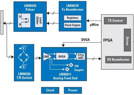
The LM96511 is an 8-channel integrated analog front end (AFE) module for multi-channel applications, particularly medical ultrasound. Each of the 8 signal paths consists of a low noise amplifier (LNA), a digitally programmable variable gain amplifier (DVGA) and a 12-bit, 40 Mega Samples Per Second (MSPS) analog-to-digital converter (ADC) with Instant Overload Recovery (IOR). The architecture of the DVGA is a digitally-controlled linear-in-dB step attenuator driving a fixed-gain post-amplifier (PA). The ADC uses a Continuous-Time-Sigma-Delta (CTΣΔ) architecture with digital decimation filtering to maximize dynamic performance and provide an alias free input bandwidth to ADC CLK / 2. The ADC digital outputs are serialized and provided on differential LVDS outputs. The ADC includes an on-chip clock cleaner PLL.
In addition, for baseband CW Doppler Beamformer applications, an 8-channel demodulator with 16 discrete phase rotation angles is included.
Selective power reduction is included to minimize consumption of idle sections during interleaved imaging modes.
An SPI™ compatible serial interface allows dynamic digital programming and control. Texas Instruments offers a full development package for sale which includes acquisition analysis hardware and software with user friendly GUI for device programming and control.
Features
- 8-Channel LNA, DVGA, and 12-bit Continuous Time ΣΔ ADC
- Programmable Active Termination LNA
- 8-channel, Integrated CW Doppler Beamforer
- Low-Power Consumption
- Embedded ADC Digital Filter
- ADC Instant Overload Recovery
- Embedded ADC “Clock-Cleaning” PLL
- 11 mm x 17 mm RoHS NFBGA Package
All trademarks are the property of their respective owners.
The Doppler block delivers 161dB/Hz of dynamic range, “enabling measurement of low velocity blood flow in organs such as the liver”, said National.
The digital variable gain amplifier (VGA), which retains an analogue signal path, significantly cuts spurious modulation of the signal compared with an all-analogue VGA, claims Ram.
“It does not spread the signal so there is more resolution and you can get low-velocity tones that otherwise the FPGA would have to extract,” he said.
To cut anti-aliasing filter requirements, the firm is noise-shaping using high-order ?? ADCs.
Sampling at 40Msample/s, the continuous time brick wall design passes 20MHz, but rejects signals above 30MHz by at least 70dB.
B-mode scan power consumption is 110mW/channel, and channel-to-channel gain matching is typically +/-0.06dB.
The LM96530 T-R switch has eight transmit-receive channels with integrated clamping diodes and individual channel shut-off.
Input referred noise is 0.5nV/?Hz and on-resistance is 16?.
To reduce the number of FPGA pins needed to operates multiple switches, controls signals can be daisy-chained between chips.
Dissipation in the switch very much depends on the application, said Ram, adding: “Typical power consumption for this performance level is in the order of 1W.”
The LM96550 transmit pulser contains eight pulsers with damper circuit that generates +/-50V pulses with peak currents up to 2A and pulse rates up to 20MHz.
Over-temperature protection is included.
Jitter from the LM96570 transmit beam former is 25ps pk-pk, which Ram claims is around 10 times better than leaving the job to the FPGA, and allows the use of a smaller FPGA.
For more read: Chipset Nat Semi for portable ultrasound scanners

