Description
The LMK04800 family is the industry’s highest performance clock conditioner with superior clock jitter cleaning, generation, and distribution with advanced features to meet next generation system requirements. The dual loop PLLatinum architecture enables 111 fs rms jitter (12 kHz to 20 MHz) using a low noise VCXO module or sub-200 fs rms jitter (12 kHz to 20 MHz) using a low cost external crystal and varactor diode.
The dual loop architecture consists of two high-performance phase-locked loops (PLL), a low-noise crystal oscillator circuit, and a high-performance voltage controlled oscillator (VCO). The first PLL (PLL1) provides a low-noise jitter cleaner function while the second PLL (PLL2) performs the clock generation. PLL1 can be configured to either work with an external VCXO module or the integrated crystal oscillator with an external tunable crystal and varactor diode. When used with a very narrow loop bandwidth, PLL1 uses the superior close-in phase noise (offsets below 50 kHz) of the VCXO module or the tunable crystal to clean the input clock. The output of PLL1 is used as the clean input reference to PLL2 where it locks the integrated VCO. The loop bandwidth of PLL2 can be optimized to clean the far-out phase noise (offsets above 50 kHz) where the integrated VCO outperforms the VCXO module or tunable crystal used in PLL1.
Features
- Ultra-Low RMS Jitter Performance
- 111 fs RMS Jitter (12 kHz to 20 MHz)
- 123 fs RMS Jitter (100 Hz to 20 MHz)
- Dual Loop PLLatinum PLL Architecture
- PLL1
- Integrated Low-Noise Crystal Oscillator Circuit
- Holdover Mode When Input Clocks are Lost
- Automatic or Manual Triggering/Recovery
- PLL2
- Normalized PLL Noise Floor of -227 dBc/Hz
- Phase Detector Rate up to 155 MHz
- OSCin Frequency-Doubler
- Integrated Low-Noise VCO
- 2 Redundant Input Clocks with LOS
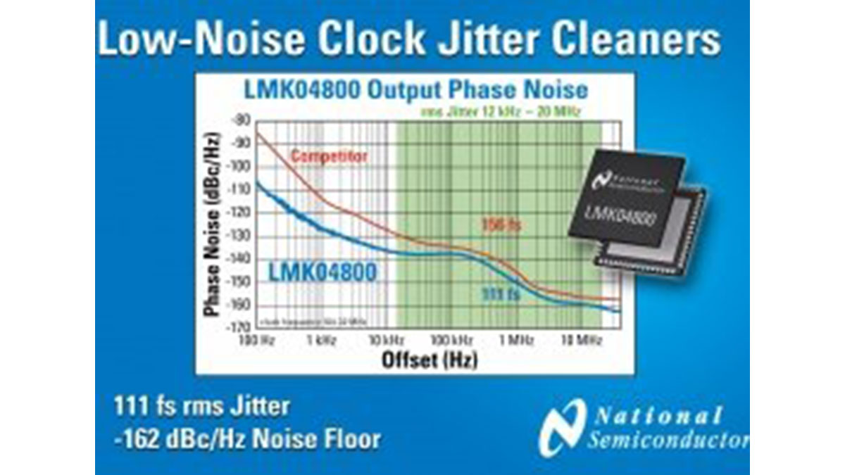
National Semiconductor claims its latest clock jitter cleaners features the industry’s lowest phase noise and rms jitter performance.
The company specifies jitter at 111 femtosecond (fs) from 12kHz to 20MHz, and a wideband noise floor of -162dBc/Hz at 184MHz output frequency.
The chip will find use in medical imaging, software defined radio (SDR) and digital broadcast applications, in particular.
The four devices in the LMK04800 family are the LMK04808, LMK04806, LMK04805 and LMK04803.
They will be used to generate different frequencies up to 1.5GHz for clocking ADCs, DACs, SerDes and FPGAs.
There are holdover and switchover functions, as well as digital and analogue delay, odd/even dividers and 12 programmable output format drivers.
For more read: Chip cleans signals clock to 111fs jitter