Summary of NXP introduces tiny mosfet in leadless package
NXP released 30V N-channel Trench MOSFETs (PMPB11EN and PMPB20EN) in a 2 x 2 x 0.6–0.65 mm DFN2020MD-6 (SOT1220) leadless ultra-thin package, offering very fast switching, exposed drain pad for thermal conduction, and tin-plated side pads for optical solder inspection; they deliver ID >10 A and Rds(on) ~12 mΩ and 16.5 mΩ (typ) at 10 V and target portable power-management applications.
Parts used in the DFN2020MD-6 MOSFET package project:
- PMPB11EN 30V N-channel Trench MOSFET
- PMPB20EN 30V N-channel Trench MOSFET
- DFN2020MD-6 (SOT1220) leadless DFN package, 2 x 2 x 0.6–0.65 mm
- Exposed drain pad (package feature)
- Tin-plated solderable side pads (package feature)
Description
N-channel enhancement mode Field-Effect Transistor (FET) in a leadless medium power DFN2020MD-6 (SOT1220) Surface-Mounted Device (SMD) plastic package using Trench MOSFET technology.
Features and benefits
- Trench MOSFET technology
- Very fast switching
- Small and leadless ultra thin SMD plastic package: 2 x 2 x 0.65 mm
- Exposed drain pad for excellent thermal conduction
- Tin-plated 100 % solderable side pads for optical solder inspection
Applications
- Charging switch for portable devices
- DC-to-DC converters
- Power management in battery-driven portables
- Hard disk and computing power management
NXP Semiconductors has introduced its first mosfet in a 2mm x 2mm low-profile DFN (discrete flat no-leads) package.
The package has tin-plated, solderable side pads which will offer the advantage of optical soldering inspection.
According to the supplier, the pads also improve solder connection compared to conventional leadless packages.
The PMPB11EN and PMPB20EN 30V N-channel mosfets are the first of more than 20 devices housed in the DFN2020MD-6 (SOT1220) package.
Both mosfets have a maximum drain current (ID) of greater than 10A, and Rds(on) values of 12mOhm typ and 16.5mOhm typ at 10V.
Package height is 0.6mm.
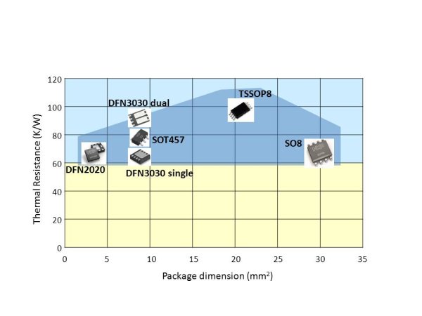
The DFN2020 package is eight times smaller than standard SO8 packages.
For more read: NXP introduces tiny mosfet in leadless package
- What is the package size of the DFN2020MD-6 MOSFETs?
The package size is 2 x 2 mm with a height of about 0.6–0.65 mm. - Which MOSFET models are introduced in this package?
The PMPB11EN and PMPB20EN 30V N-channel MOSFETs are introduced in this package. - What technology is used in these MOSFETs?
They use Trench MOSFET technology. - What are the typical Rds(on) values at 10 V?
Typical Rds(on) values are 12 mOhm and 16.5 mOhm at 10 V. - What is the maximum drain current capability?
Both MOSFETs have a maximum drain current greater than 10 A. - What package features improve thermal and soldering performance?
An exposed drain pad improves thermal conduction and tin-plated side pads allow optical solder inspection and improved solder connection. - What applications are targeted for these MOSFETs?
They target charging switches for portable devices, DC-to-DC converters, power management in battery-driven portables, and hard disk and computing power management. - How does the DFN2020 package size compare to SO8?
The DFN2020 package is eight times smaller than standard SO8 packages.