
Summary of LTC3265 – Low Noise Dual Supply with Boost and Inverting Charge Pumps
The LTC3265 is a low-noise dual polarity power supply featuring boost and inverting charge pumps paired with positive and negative LDO post-regulators. It supports input voltages up to 16V for the boost pump and 32V for the inverting pump, delivering up to 50mA per regulator. The device offers programmable oscillator frequencies (50kHz–500kHz), operates in Burst Mode or constant frequency modes, and includes short-circuit and thermal protection in compact DFN and TSSOP packages.
Parts used in the LTC3265 Project:
- Boost Charge Pump
- Inverting Charge Pump
- Low Noise Positive LDO Post Regulator
- Low Noise Negative LDO Post Regulator
- External Resistor Dividers
- External Timing Resistor
- Ceramic Capacitors
- 18-Lead DFN Package
- 20-Lead TSSOP Package
Features
- Boost Charge Pump Generates 2 • VIN_P (VIN_P Range: 4.5V to 16V)
- Inverting Charge Pump Generates –VIN_N (VIN_N Range: 4.5V to 32V)
- Low Noise Positive LDO Post Regulator Up to 50mA
- Low Noise Negative LDO Post Regulator Up to 50mA
- 135μA Quiescent Current in Burst Mode® Operation with Both LDO Regulators On
- 50kHz to 500kHz Programmable Oscillator Frequency
- Stable with Ceramic Capacitors
- Short-Circuit/Thermal Protection
- Low Profile 3mm × 5mm 18-Lead DFN and Thermally Enhanced 20-Lead TSSOP Packages
Description
The LTC®3265 is a low noise dual polarity output power supply including a boost charge pump, an inverting charge pump and two low noise positive and negative LDO post regulators. The boost charge pump powers the positive LDO post regulator while the inverting charge pump powers the negative LDO regulator. Each LDO can provide up to 50mA of output current. The LDO output voltages can be adjusted using external resistor dividers.
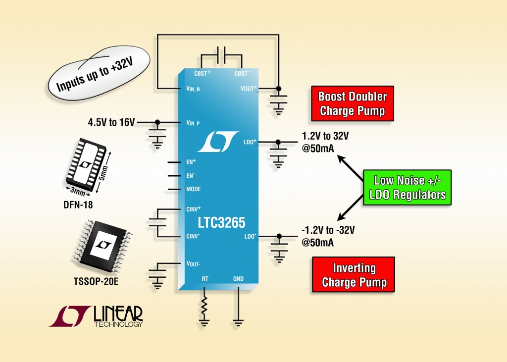
The charge pumps employ low quiescent current Burst Mode operation or low noise constant frequency mode. During Burst Mode operation, the boost charge pump regulates its output (VOUT +) to 0.94 • 2 • VIN_P while the inverting charge pump regulates its output (VOUT –) to –0.94 • VIN_N. In Burst Mode operation the LTC3265 draws only 135μA of quiescent current with both LDOs on. In constant frequency mode, the boost and inverting charge pumps produce outputs equal to 2 • VIN_P and –VIN_N respectively and operate at a fixed 500kHz or to a programmed value between 50kHz to 500kHz using an external resistor. The LTC3265 is available in low profile 3mm × 5mm × 0.75mm 18-lead DFN and thermally enhanced 20-lead TSSOP packages.
Applications
- Low Noise Bipolar/Inverting Supplies
- Industrial/Instrumentation Low Noise Bias Generators
For More Details: LTC3265 – Low Noise Dual Supply with Boost and Inverting Charge Pumps
-
What output voltage does the boost charge pump generate?
The boost charge pump generates 2 • VIN_P with an input range of 4.5V to 16V. -
How much current can each LDO regulator provide?
Each LDO can provide up to 50mA of output current. -
Can the LDO output voltages be adjusted?
Yes, the LDO output voltages can be adjusted using external resistor dividers. -
What is the quiescent current during Burst Mode operation?
The device draws only 135μA of quiescent current with both LDOs on during Burst Mode. -
How is the oscillator frequency programmed?
The frequency is programmed between 50kHz to 500kHz using an external resistor. -
Does the LTC3265 operate stably with ceramic capacitors?
Yes, the device is stable with ceramic capacitors. -
What protection features are included in the device?
The device includes short-circuit and thermal protection. -
Which package options are available for the LTC3265?
It is available in a low profile 3mm × 5mm 18-lead DFN and a thermally enhanced 20-lead TSSOP.
