General Description
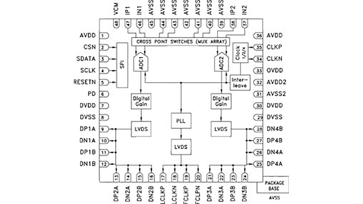
The HMCAD1512 is a versatile high performance low power analog-to-digital converter (ADC), utilizing time-interleaving to increase sampling rate. Integrated Cross Point Switches activate the input selected by the user.
The device contains 2 ADCs that can be interleaved by the user to act as a single channel or two channels. In single
channel mode, either of the two inputs can be selected as a valid input to the single ADC channel. In dual channel
mode, either of the two inputs can be selected for each ADC channel. (The HMCAD1512 does not support the quadchannel mode. The HMCAD1511 should be used for this purpose).
An internal, low jitter and programmable clock divider makes it possible to use a single clock source for all operational modes.
The HMCAD1512 is based on a proprietary structure, and employs internal reference circuitry, a serial control interface and serial LVDS/RSDS output data. Data and frame synchronization clocks are supplied for data capture at the receiver. Internal 1 to 50X digital coarse gain with ENOB > 7.5 up to 16X gain, allows digital implementation of oscilloscope gain settings. Internal digital fine gain can be set separately for each ADC to calibrate for gain errors.
Various modes and configuration settings can be applied to the ADC through the serial control interface (SPI). Each
channel can be powered down independently and data format can be selected through this interface. A full chip idle
mode can be set by a single external pin. Register settings determine the exact function of this pin.
HMCAD1512 is designed to easily interface with Field Programmable Gate Arrays (FPGAs) from several vendors.

Features
• 8-bit High Speed Single/ Dual ADC
Single Channel Mode: FSmax = 900 MSPS
Dual Channel Mode: FSmax = 450 MSPS
• Integrated Cross Point Switches (Mux Array)
• 1X to 50X digital gain
No missing codes up to 32X
• Internal low jitter programmable Clock Divider
• Ultra Low Power Dissipation
650 mW including I/O at 900 MSPS
• 0.5 μs start-up time from Sleep,
15 μs from Power Down
• Internal reference circuitry with no
external components required
• Coarse and fine gain control
• Digital fine gain adjustment for each ADC
• Internal offset correction
• 1.8 V supply voltage
• 1.7 – 3.6 V CMOS logic on
control interface pins
• Serial LVDS/RS DS output
• 7×7 mm QFN 48 Pin (LP7D) Package
Hittite Microwave has introduced a two channel 8bit 450Msample/s ADC with interleaving for 900Msample/s conversion, from either input.
Called HMCAD1512, it is aimed at point-to-point microwave links and digital oscilloscopes.
At full speed operation, a signal-to-noise ratio of 49dB (full scale) is to be expected with a 170MHz input.
Power dissipation
“Total power dissipation at full speed operation is only 650mW, including I/O,” said the firm. “This performance to power ratio makes the part a perfect choice for low power high performance devices, including handheld and portable test equipment.”
Internal resolution is 13bit “providing a digital gain of 1X to 50X”, said Hittite. “Subsequently, the full scale range of operation can be varied from 2Vp-p down to 63mVp-p.
For more read: 8bit 450/900Msample/s ADC claims better SNR/Watt
