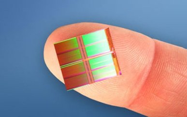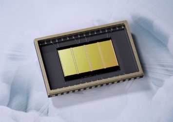
NAND scaling issues becoming more complex
NAND process geometries have become as problematic as logic process geometries with the advantages of further scaling – especially as 3D NAND approaches – being questioned. NAND process geometry is currently at 20nm and should be 10-20nm in 2017, says IC Insights adding “reported minimum feature sizes and mass production definitions are very imprecise and […]
NAND scaling issues becoming more complex Read More »