Summary of Samsung Finding U.S. Lab to Advance its 3-D FinFET to 5nm
Samsung funds Penn State researchers to fabricate III-V indium gallium arsenide FinFETs for 7nm and 5nm nodes. The project utilizes a novel five-gate structure grown on indium phosphide substrates to prove high mobility at low voltages, though future integration requires solving challenges in moving these materials to standard silicon wafers.
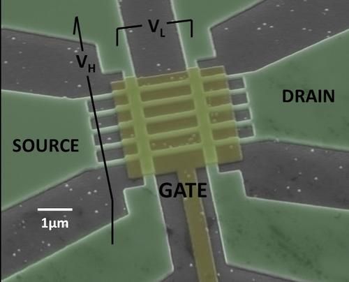
Parts used in the Samsung Indium Gallium Arsenide FinFET Project:
- Samsung funding
- Penn State University researchers
- III-V indium gallium arsenide (InGaAs) FinFETs
- Five-gate structure
- Indium phosphide (InP) substrate
- Materials Research Institute's Nanofabrication Laboratory
- 12-inch (300mm) silicon substrates
PORTLAND, Ore. — Samsung is funding Pennsylvania State University researchers working to fabricate III-V indium gallium arsenide FinFETs for possible use at the 7nm node.
The silicon FinFET (3D fin gates on field effect transistors) have become the standard for low leakage and high performance at advanced nodes, but III-V compounds such as indium gallium arsenide (InGaAs) are faster than silicon, prompting researchers at Penn State to combine the best of both worlds. Penn State’s InGaAs FinFET transistors use a novel five-gate structure grown on an indium phosphide (InP) substrate in its Materials Research Institute’s Nanofabrication Laboratory.
“These FinFETs as of now have been fabricated on InP substrates,” Arun Thathachary, a EE doctoral candidate working under professor Suman Datta, told us. “Samsung will own the IP generated from this project.” Fellow doctoral candidate Nidhi Agrawal has also contributed to the project.
For years, other semiconductor firms have funded research to fabricate III-V transistors on silicon substrates, including Intel, Sematech, and, more recently, Imec.
The reason everybody is trying to integrate III-V transistor channels with silicon substrates is cost. Not only are InP wafers more expensive, but the entire semiconductor industry is based on equipment optimized for silicon manufacturing. So even though Penn State is using InP wafers to prove the concept that III-V FinFETs will retain their high mobility at advanced nodes (5 nm) and at lower voltages (0.5 V), Samsung would eventually have to solve the problems of integrating III-V materials with complementary (n- and p-channel) metal-oxide semiconductors (CMOS) on 12-inch (300mm) silicon substrates.
Thathachary told EE us:
This entire research project is being sponsored by Samsung with the sole purpose of investigating III-V materials for low-power CMOS manufacturing. But as far as integration on 300-millimeter silicon goes, there are significant growth challenges involved in engineering the buffer layers. Though there have been several publications in this regard over the last couple of years, a high-yield solution for 300-millimeter manufacturing is still lacking.
For more detail: Samsung Finding U.S. Lab to Advance its 3-D FinFET to 5nm
- Who is funding the research?
Samsung is funding Pennsylvania State University researchers working on this project. - What type of transistors are being fabricated?
The team is fabricating III-V indium gallium arsenide FinFETs. - On what substrate were the initial FinFETs built?
The FinFETs have been fabricated on indium phosphide substrates. - Why are companies trying to integrate III-V transistors with silicon?
The primary reason is cost, as InP wafers are more expensive and equipment is optimized for silicon. - What node sizes is this technology targeting?
The research targets the 7nm node and aims to retain performance at advanced 5 nm nodes. - Who owns the intellectual property generated from this project?
Samsung will own the IP generated from this project. - What specific challenge exists for 300-millimeter manufacturing?
There are significant growth challenges involved in engineering buffer layers for high-yield solutions. - At what voltage does the technology aim to operate?
The research demonstrates high mobility at lower voltages of 0.5 V.