The purpose of a PLL is to generate a frequency and phase-locked output oscillation signal.
To accomplish this objective, past methods primarily worked by adjusting the PLL output frequency often based on the phase error (i.e. the faster/slower phase relationship) to produce a temporary, non-constant frequency and phase-locked output oscillation signal. The constant fluctuation in VCO frequency leads to noticeable Jitter and extended settling time as the correct phase often coincides with an incorrect frequency, and vice versa.
1. Field of the Invention
The current invention pertains to Phase Locked Loops (PLL), which utilize both voltage-controlled oscillators (VCO) and digital-controlled oscillators (DCO).
2. Description of Prior Art
Analog phase-locked loops typically consist of a phase detector, a low-pass filter, a voltage-controlled oscillator, and a frequency divider arranged in a negative feedback setup.
Digital phase-locked loops typically consist of a time-to-digital converter, a digital loop filter, a digitally controlled oscillator (DCO), and a frequency divider within a negative feedback setup.
A VCO or DCO efficiently provides oscillation waveform with variable frequency. PLL synchronises VCO / DCO frequency to input reference frequency feedback.
VCO output frequency Fvco = Kvco * Vctl, where Kvco is constant gain over most of the usable control voltage range, and Vctl is VCO control voltage.
A crucial component of a PLL is the phase detector or time-to-digital converter. This involves comparing the phase of both inputs to the detector and generating a corrective voltage signal to regulate the oscillator to achieve zero phase difference between the inputs. Normally, the phase detector receives input from the reference signal and the divided VCO or DCO output.
The purpose of PLL is to generate a frequency and phase locked output oscillation signal.
However, prior art cannot achieve the desired purpose because (1) VCO and DCO are frequency variable and controllable, they are not phase variable and controllable and (2), using phase error to correct frequency is improper because it is a conflict control and leads to infinite jitter in PLL output (i.e. deviation of VCO/DCO output edges from their ideal placement in time). Due to these two reasons, neither frequency nor phase will actually be locked – making PLL performance difficult to improve.
Prior art essentially functioned by frequently changing the PLL output frequency according to the phase error (i.e. the faster/slower phase relationship) to generate a momentary, but not static, frequency and phase locked output oscillation signal. This change in VCO frequency creates significant jitter and a longer settling time.
Summary of the Invention
A perfect PLL should produce a highly consistent output oscillation signal with a genuinely locked frequency, and a genuinely locked phase (meaning both frequency and phase remain constant over time).
Two signals must have identical frequencies or be within a small range of each other to achieve true phase locking where their phase remains constant over time.
This can be more clearly explained by following mathematical equations.
Let ∆Φ(t) = relative phase error, ω1 = frequency1, ω2 = frequency2, (ω1- ω2) = frequency error, θ1 is ω1’s initial phase (constant), θ2 is ω2’s initial phase (constant), and t = time,
Ref(t) = M * sin (ω1*t + θ1) = M * sin (∆θ1(t)+ θ1), (1-1)
Div(t) = N * sin (ω2*t + θ2) = N * sin (∆θ2(t)+ θ2), (1-2)
∆Φ(t) = (ω1- ω2)*t +(θ1 – θ2) = (∆θ1(t) – ∆θ2(t)) +(θ1 – θ2), (1-3)
According to equation (1-3), at any time, when ω1= ω2 or (ω1- ω2) = 0, ∆Φ(t) = θ1 – θ2 becomes a constant, the two signals will have a fixed phase relationship and, therefore, no jitter, otherwise, relative phase error ∆Φ(t) will change with t, ω1 or ω2 – meaning that the distance between Ref(t) ’s and Div(t)’s rising or falling edges will change with time and therefore, jitter will happen.
Prior art (faster/slower feedback control) can be expressed by the following advanced mathematical equation.
∆Φ(t) = ∫∆ω(t)*dt = ∫(ω1(t)- ω2(t))*dt
when phase is locked, mathematically, ∆Φ(t) ≈ constant (even ω1(t) – ω2(t) ≠ 0, the integral result ∆Φ(t) is still possible to be a constant). But in reality, ∆Φ(t) will change (within a narrow, allowable range) with t, ω1(t) or ω2(t). That is why jitter will be inevitable.
The new method in this invention changes the single loop PLL with a frequency-locked loop and a phase-locked loop. The frequency loop is controlled by frequency error, while the phase-locked loop is controlled by dynamic phase error rather than static phase error. The frequency-locked loop targets a frequency variable unit/device such as VCO and DCO. The phase-locked loop’s controlling goal is a unit/device that can vary in phase delay. Furthermore, it offers an enhanced proportional and integral feedback control method and a basic but effective frequency error detector for the mentioned frequency-locked loop. Thirdly, it offers a flexible phase error identification and rectification for the mentioned phase-locked loop.
The current invention offers various benefits: enabling separate control over frequency and phase, achieving true locking with minimal error (ideally zero), reducing jitter significantly (without utilizing phase error for VCO or DCO control), providing swift output response with minimal or no frequency overshot/undershot, and ensuring high-frequency precision when locked, all while maintaining a straightforward design that is simple to manufacture.
Preferred Embodiment
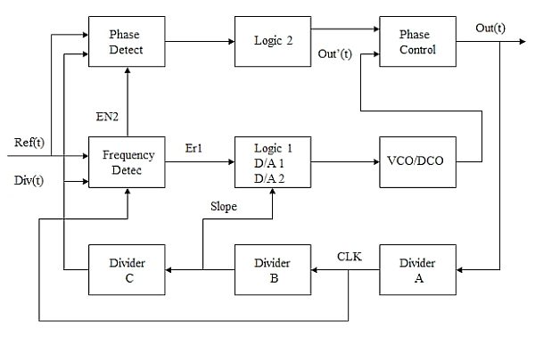
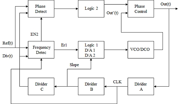
In Figure 1, a frequency-locked loop is built of frequency detect, logic 1, D/A1, D/A2, VCO/DCO, phase control, Divider A, Divider B, and Divider C.

A phase locked loop is built of phase detect, logic 2, phase control, Divider A, Divider B, and Divider C.
A frequency and phase locked loop is built of connecting the output of the frequency locked loop Out’(t) with the input of the phase locked loop to output a frequency and phase locked signal Out(t).
In the frequency locked loop, Out(t) is first divided by Divider A to generate a signal CLK. CLK is provided to Divider B for further dividing and to frequency detect as high speed sampling clock for Ref(t) and Div(t). The output of Divider B generates a signal slope. Slope is provided to the logic, D/A1, D/A2 as a clock of a counter used for frequency coarse tune and to Divider C for further dividing. Because the frequency of signal slope will determine the rising speed of the counter’s outputs which are converted to a frequency control voltage by D/A1 for frequency proportional/coarse control, it is named slope.
Changing Divider B can change the slope of proportional frequency control. Divider C generates signal Div(t). Div(t) is provided to frequency detect where its frequency is compared with and subtracted by reference signal Ref(t). Frequency detect generates a frequency error signal Er1 and an enable signal EN2. Er1 is the frequency difference / error between Ref(t) and Div(t) and is provided to logic 1, D/A1, D/A2 for setting the D/A1’s output at the end of proportional control (coarse tune)and for D/A2’s integral control (fine tune) so that Er1 will be or approximate to zero and frequency can be locked. EN2 is an enable signal which will become ‘1’ when frequency is locked and is provided to phase detect to enable phase error detect.
The output of logic 1, D/A1, D/A2 block is provided to control VCO/DCO. The output of VCO/DCO , Out’(t) is a frequency locked signal which is provided to phase control. The output of phase detect is provided to Logic 2. Logic 2 generates a phase control signal which decides whether to increase or decrease phase delay and is provided to phase control. Phase control will add or subtract delay to the VCO/DCO output signal Out’(t) accordingly and output a frequency and phase locked signal Out(t).
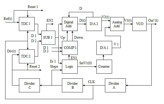
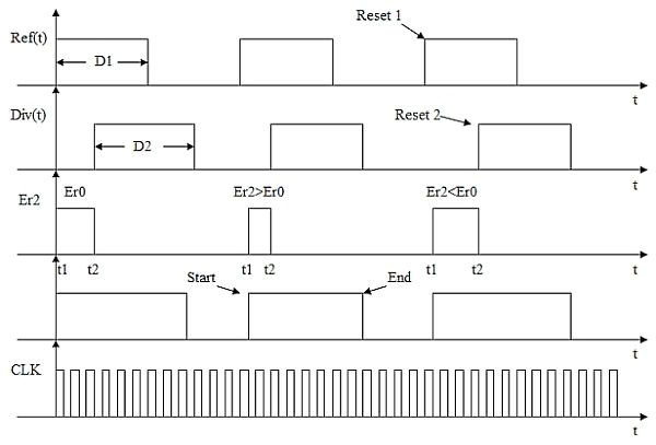
In Figure 2, TDC1 and TDC2 comprise two identical counters which will be reset at Ref(t) and Div(t) rising edges respectively, then start to count CLK and stop at Ref(t) and Div(t) falling edges respectively. Referring to Figure 4, at the end, TDC1’s output is the CLK pulse numbers counted during D1, TDC2’s output is the CLK pulse numbers counted during D2. In this way, high resolution time to digital conversions are achieved (D1 and D2 can have phase difference).

SUB1 receives digitized inputs D1 and D2. SUB1 takes the difference between D1 and D2, providing the absolute value as Er1 frequency error, and triggers EN2 high when Er1 reaches zero for the first time. Er1 is given for digital addition and logic functions. In logic, the initial rising edge from Er1 will produce a start signal to begin coarse tune/proportional frequency control and activate the counter. At the same time, the starting output value of D/A2 is configured to be half of its highest value. The counter is designed as a pre-set up/down counter, where it counts down if the current value is higher than the pre-set one, counts up if lower, and stops if they are equal.
The preset counter value is determined by the target frequency and control voltage of the VCO/DCO and is adjusted at the beginning of each coarse tune. When the counter reaches its pre-set value, the logic will produce a stop signal to finish the coarse tune and halt the counter, while also sending a high EN1 signal to COMP1 to start the fine-tune/integral frequency control. The counter will maintain its output value to create an output voltage V1 through D/A1 to achieve a coarse adjustment. V1 is given for analog addition. Once EN1 is activated, COMP1 checks if D1 is greater than, less than, or equal to D2, generating corresponding up, down, or both signals accordingly.
Digital ads receive both upward and downward signals. In digital addition, the current value Er1 is added/subtracted to the previous output value D read back from D/A2 based on the up/down signal. The outcome will be utilized to revise D and produce the following V2(t). This procedure will persist until Er1 reaches zero or falls within an acceptable range. The analog add receives the output, V2(t), from D/A2. Analog combines V2 with V1 to create a proportional and integral frequency control voltage V1 for VCO/DCO. VCO produces an output signal Out'(t) that is locked to a frequency when Er1 equals zero.
Since TDC1 and TDC2 are the same and share the same clock signal, any timing errors from the clock can be mostly eliminated by SUB1 (even with a phase difference). When D1 and D2 are equal, this will result in a very reliable frequency error Er1, so there is no need for an extra ring oscillator to create the clock signal. This will greatly streamline design while offering high resolution, minimal error time for digital conversion even during loop transient period.
When EN2 goes high, AND2 is chosen as the initial delay selection. SUB2 will transform the time gap between Reset1/t1 and Reset2/t2 into a digital constant phase error denoted as Er2. The initial static phase error/first Er2 value will be stored in SUB2’s register as Er0, to be used as a benchmark for future comparisons. COMP2 is given Er2. COMP2 will produce an up signal high if Er2 is lower than Er0, a down signal high if Er2 is higher than Er0, and both signals low if Er2 equals Er0. The upcoming Er2 value will be compared to Er.

SHIFT Reg receives signals that go both upwards and downwards. If both the up event and up signals are high, AND3 will be chosen to introduce a delay to Out’(t); if both the down event and down signals are high, AND1 will be chosen to decrease the delay to Out’(t); if both the up and down signals are low, there will be no alteration. Just one AND gate will be chosen out of the three options. This ensures that the relative phase difference between Ref(t) and Div(t) stays near Er0 or is locked. As a result, Out(t) is locked in frequency and phase. Adding more delay stages can enhance the precision of the phase-locked loop. There is no requirement to eliminate the static phase error Er0 to zero when using PLL as a frequency synthesizer. However, if needed, the static phase error Er0 can be reduced to zero by synchronizing the VCO output with D1’s rising or falling edge after both frequency and phase are locked, while also ensuring Er0 is set to zero.
Once the frequency is set, whenever the phase goes beyond the control limit, frequency fine-tuning will be activated. In case of a change in frequency band, the coarse tune will start and a different pre-set value will be given to the counter.
The diagrams shown here are simply illustrations. There could be numerous modifications to these diagrams or the steps (or operations) explained here without losing the essence of the invention. All of these different versions are seen as belonging to the invention that has been claimed.
Even though the main version of the innovation has been explained, it is acknowledged that experts in the field, both currently and in the future, can introduce different enhancements that are covered by the following claims.
These claims should be construed to maintain the proper protection for the invention first described.
I claim:
- Frequency and Phase-locked Loops for controlling the frequency and phase of an output signal Out(t) in response to an input signal Ref(t), comprising:
(a) A frequency feedback control loop for controlling the frequency of an output signal Out(t) in response to an input Ref(t) signal frequency according to a frequency error Er1 between its divided output signal Div(t) and input signal Ref(t) and for generating an EN2 high signal to initiate phase feedback control when frequency error Er1 becomes zero or frequency is locked.
(b) A phase feedback control loop for controlling the phase of a divided output signal Div(t) in alliance to/to match with an input signal Ref(t) phase according to the first static phase error Er0 between its divided output signal Div(t) and input signal Ref(t) and to the phase error between the first static phase error Er0 and the subsequent static phase error Er2 and for initiating frequency integral control when phase control is out of range. - The apparatus of claim 1, where in said frequency feedback control loop comprises: An open proportional control loop and a close integral control loop.
- The apparatus of claim 2, where in said open proportional control loop comprises: Means for changing the slop and controlling the time length of proportional control and for initiating frequency integral control when counter’s output value is equal to its pre-set value.
- The apparatus of claim 3, where in said means for changing the slope comprises: To change slope by changing Divider B’s constant dividing value.
- The apparatus of claim 3, where in said means for controlling the time length of open loop proportional control comprises: Logic generates an EN1 high to hold proportional control and to enable frequency integral control when up/down counter’s output value becomes equal to its pre-set value.
- The apparatus of claim 2, where in said close loop frequency integral control comprises: Means for frequency error Er1 generation and integral control.
- The apparatus of claim 6, where in said frequency error generation comprises: Using a high frequency CLK from the feedback Divider A to drive two identical counters combining with logic control within TDC1 and TDC2 to achieve time to digital conversion, to generate a frequency error Er1 and to generate an EN2 high signal to initiate phase feedback control after Er1 becomes zero.
- The apparatus of claim 6, where in said close loop frequency integral control comprises: Means for adding or subtracting the next frequency error Er1 with previous result D and updating D.
- The apparatus of claim 1, where in said phase feedback control loop comprises: Means for using first static phase error of Er2 value as a reference phase error Er0 to compare with subsequent Er2 to add or subtract phase delay to frequency feedback loop’s input signal Out’(t) and output a frequency and phase locked signal Out(t).
Source: Frequency and Phase Locked Loops (PLL)

