PORTLAND, Ore. — Complementary metal oxide semiconductor (CMOS) imaging chips are becoming the industry’s leader in advanced process technology — instead of the traditional leaders (processors and memory) — thanks to strong demand for CMOS imaging chips in everything from smartphones to tablets to medical equipment and automobiles. Apparently, now the innovation surpasses Moore’s Law, says analyst firm Yole Développement.

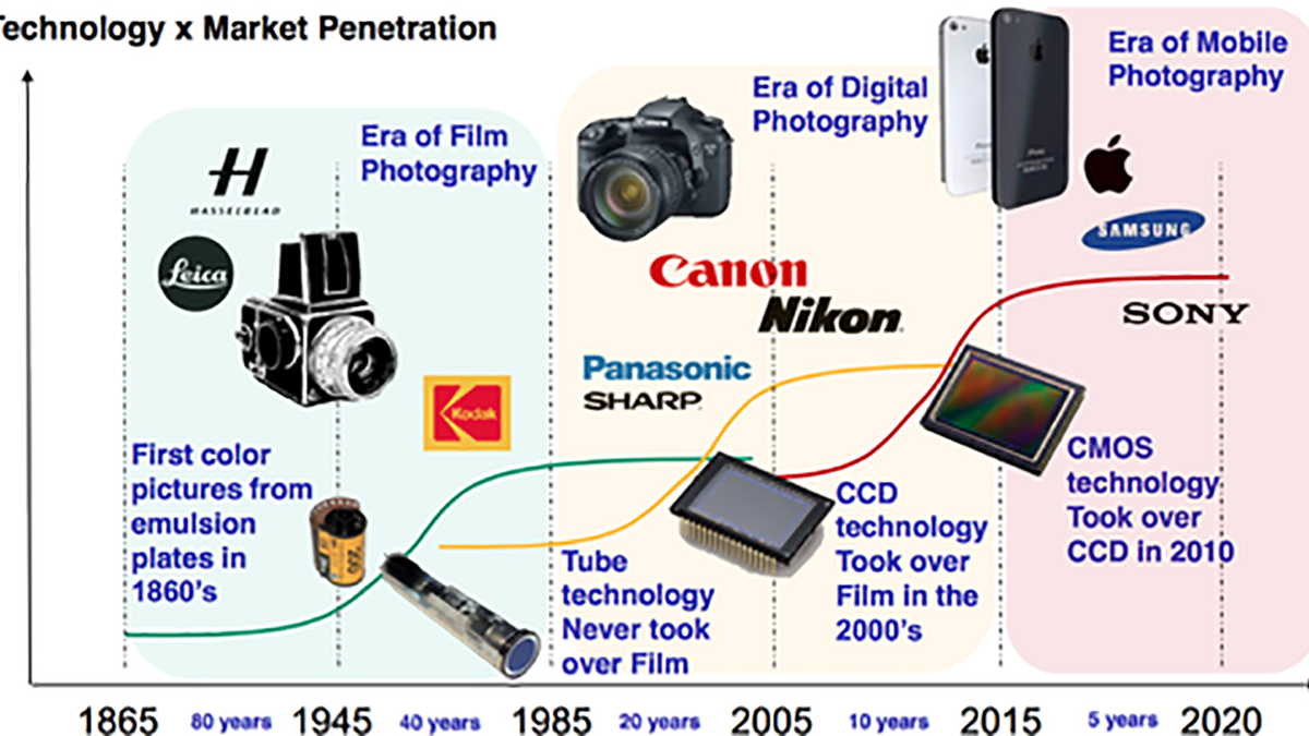
Imaging was once done by film, but with the advent of solid-state sensors the technology breakthroughs seem to be growing exponentially, doubling with each new innovation (see slide 1), thus surpassing the traditional interpretation of Moore’s Law, argues Yole Développement (Lyon, France) in a new paper. Yole calls this effect “More than Moore.”
At the pinnacle of this growth is 3-D stacking, the allure of which for imaging chips is downsizing the chip while simultaneously packing more pixels per unit size, thus one-upping processors and memory, which are only now perfecting the through-silicon-via (TSV) notably with Micron’s Hybrid Memory Cube. CMOS imaging chips, however, are one-step-ahead perfecting copper-to-copper bonding of wafers containing the interconnection metallization for pixel arrays and the digital processing layers of the imaging chip on separate layers below the top (pixel) level.
“The interconnection between the upper part of the 3D stack and the lower part is currently done using TSVs. Two vias are needed for each connection and act as a bridge between the two layers. The metal connection between the two vias is done at the surface of the chip,” Pierre Cambou told EE Times, co-author of “Status of the CMOS Image Sensors Industry” with Jean-Luc Jaffard, both Yole Développement analysts.
For More Details: CMOS Image Sensors Surpassing Moore’s Law
