1. Introduction
As the portable electronics industry has advanced over the years, various requirements have emerged, including longer battery life, smaller and more affordable systems, brighter full-color displays, and increased talk time for cellular phones. The growing demand for power systems has made power consumption a critical concern. To meet these demands, engineers have focused on developing efficient conversion techniques, leading to the formal growth of the interdisciplinary field of power electronics. This field combines three major disciplines of electrical engineering: electronics, power, and control, presenting unique challenges. It involves control theory, filter synthesis, signal processing, thermal control, and magnetic component design.
This section summarizes the motivation and background work for the thesis, as well as our contributions and the outline of the thesis.
TYPES OF CONVERTERS
- AC-AC converter
- DC-DC converter
- AC-DC converter
DC-AC converter:-
An AC-AC converter, also known as a cycloconverter, transforms an AC waveform, such as the mains supply, into another AC waveform with arbitrarily adjustable output voltage and frequency.
The input to a cycloconverter is typically a single-phase or three-phase AC mains supply with fixed voltage and fixed frequency. The cycloconverter produces an output with variable voltage and variable frequency, where the output frequency is lower than the input frequency. Cycloconverters are primarily used in AC traction drives.
DC-AC CONVERTER:-
A DC-AC converter, commonly known as an inverter, is an electrical device that converts direct current (DC) into alternating current (AC). The AC output can be adjusted to any required voltage and frequency using appropriate transformers, switching, and control circuits. The inverter essentially performs the reverse function of a rectifier.
There are two main types of inverters:
- Modified sine wave
- Pure sine wave
A modified sine wave inverter produces an output that resembles a square wave, except the output goes to zero volts briefly before switching to positive or negative. In contrast, a pure sine wave inverter generates a nearly perfect sine wave output, closely resembling the power supplied by the utility grid.
AC-DC CONVERTER:-
A device that converts AC voltage to DC voltage is called a rectifier. It is an electrical device that transforms alternating current (AC), which periodically reverses direction, into direct current (DC), which flows in only one direction. This process is known as rectification.
DC-DC CONVERTER:-
A DC-to-DC converter, also known as a chopper, is an electronic circuit that converts direct current (DC) from one voltage level to another. It is a type of power converter.
DC-to-DC converters are essential in portable electronic devices such as cellular phones and laptops, which primarily rely on battery power. Most DC-to-DC converters regulate the output voltage. Exceptions include high-efficiency LED power sources, which regulate the current through LEDs, and simple charge pumps that double or triple the input voltage.
DC-to-DC converters efficiently provide a fixed output voltage by converting the input voltage. There are three main types:
- Step-up DC/DC converters
- Step-down DC/DC converters
- Step-up/down DC/DC converters
Currently, DC/DC converters can be categorized into two broad groups:
- Non-isolated DC/DC converters
- Isolated DC/DC converters
NON-ISOLATED DC/DC CONVERTERS
A non-isolated converter typically uses an inductor and does not provide DC voltage isolation between the input and output. Most applications do not require DC isolation between input and output voltages, making non-isolated DC-DC converters suitable for a wide range of uses. These converters have a direct DC path between their input and output.
One major application for non-isolated DC-DC converters is in battery-based systems that do not utilize AC power lines. Another common application is point-of-load DC-DC converters, which draw input power from an isolated DC-DC converter, such as a bus converter.
Most of these DC-DC converter integrated circuits (ICs) use either an internal or external synchronous rectifier. Their only magnetic component is usually an output inductor, making them less prone to generating electromagnetic interference. Compared to isolated DC-DC converters, non-isolated converters are generally less expensive, have fewer components, and require less PCB area for the same power and voltage levels. Non-isolated buck converters are often used for lower voltages (e.g., 12V).
ISOLATED DC/DC CONVERTERS
For safety reasons, electronic systems must have isolation between the AC input and the DC output. This requirement applies to all systems operating from the AC power line, often achieved through an isolated front-end AC-DC power supply followed by an isolated “brick” DC-DC converter and a non-isolated point-of-load converter. Depending on the application, typical isolation voltages for AC-DC and DC-DC power supplies range from 1500 to 4000V. An isolated converter uses a transformer to provide DC isolation between the input and output, eliminating the direct DC path between them. These converters utilize a switching transformer whose secondary side is either diode-rectified or synchronous-rectified to produce a DC output voltage, typically filtered by an inductor-capacitor output filter. This configuration can generate multiple output voltages by adding secondary transformer windings.
Modern electronic devices demand efficient, high-quality, and lightweight power supplies. Linear power regulators, which operate based on current or voltage division, are inefficient and primarily used for low power levels. For higher power levels, switching regulators are preferred, as they operate with switches in on and off states. Advanced power electronic switches can operate at high frequencies, enabling a faster dynamic response to rapid changes in load current. These high-frequency electronic power processors are crucial for DC-DC power conversion.
The main functions of DC-DC converters include:
- Converting DC input voltage into DC output voltage.
- Providing isolation between the source and load.
- Regulating the output voltage against varying loads.
- Reducing AC voltage ripple on the DC output voltage.
DC-DC converters are categorized into two main types:
- Hard switching pulse width modulated (PWM) converters.
- Resonant and soft switching converters.
This thesis focuses on PWM DC-DC converters, which have been popular for several decades and are used across all power levels.
Certain applications impose additional technical constraints. For instance, power supplies for battery-powered electronics like laptops and mobile phones must maintain high efficiency across a wide range of loads. In desktop computers and servers, microprocessor supplies need digitally programmable output voltage, dependent on the load, with a fast dynamic response even for significant load transients. Voltage Regulator Modules (VRMs) often feature multi-phase architectures with several buck or similar converter modules operating in parallel to share the load current, enhancing dynamic response.
The wide range of applications in industries, the telecom sector, and the medical field has driven the development of “Digital Power,” leading to the computerization of DC-DC converters, which is a key focus area today. Enhanced performance can be achieved through modeling and simulation of the system. The modeling relies on the internal structure of the system, and system dynamics are influenced by the load. Insufficient information about system parameters can lead to design errors in the controller. Better control can be achieved using experimental data to determine load information.
System identification can be done in two ways: Parametric and Non-parametric identification. In the Non-parametric method, spectral analysis and correlation analysis are used to estimate the frequency response or impulse response of the system, from which the system’s behavior is inferred. In parametric estimation, a model structure is proposed, and the model’s parameters are identified using information extracted from the system. This paper employs the Non-parametric system identification method.
2. Boost Converter
2.1 BOOST CONVERTER
In this section, we provide a brief introduction to the boost converter, explain why we chose this type of converter, and discuss its circuit topology and the components used in its construction.
Recent years have seen remarkable advancements in electrical components, driven by the demand for portability and flexibility, making devices more convenient and efficient. Power consumption is a critical factor in the operation of electrical components, and DC-DC converters play a crucial role in optimizing their usage. These converters are widely employed in various electronic devices, including telecommunication equipment, due to their ability to step up voltage and regulate it for electronic circuits.
2.2 Why Boost Converter?
In general, a boost converter is the simplest method to increase the voltage of a DC supply, which is not achievable using transformers, while also ensuring high efficiency. Consider the linear regulator shown in Figure 1. In this setup, the source voltage Vs needs to be stepped down to the voltage VL across resistor R1, resulting in a voltage drop across RL and consequently wasting power as heat. This issue can be resolved by using a boost converter, which operates using a switch (diode) that alternates between ON and OFF states.
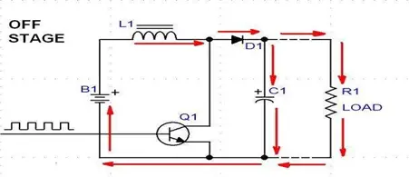
The DC-DC boost converter topology is widely utilized in power management and microprocessor voltage-regulator applications. These applications demand high frequency and rapid response to transient changes across a broad load current spectrum. Boost converters excel in converting high voltages into regulated lower voltages. They find application in computers where voltage needs to be stepped down efficiently. Boost converters also extend battery life in mobile phones that spend extended periods in standby mode.
During operation, when the switch is ON, the inductor charges up to its maximum capacity. The converter then switches to the OFF state to manage this charge effectively. This capability eliminates the need for heat sinks and cooling agents, making boost converters preferable over linear regulators due to their efficiency advantages.
2.3 Boost Converter Circuit topology
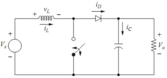
The term “Boost Converter” itself indicates that it increases the input voltage, resulting in a higher voltage at the output. A boost converter, or step-up voltage regulator, offers non-isolated, switch-mode DC-DC conversion with the advantages of simplicity and cost-effectiveness. Figure 2 illustrates a simplified DC-DC boost converter that takes a DC input and uses pulse width modulation (PWM) at the switching frequency to regulate the output voltage. Components typically include the source voltage Vs, a diode, an inductor L, inductor resistance RL, a capacitor C, and capacitive resistance Rc, all connected to a load.
Switch-mode power supplies are commonly employed to deliver output voltages higher than the input voltage to loads from an intermediate DC bus or battery source. Figure 3 depicts a simplified point-of-load boost converter where the power supply is derived from a switch-mode buck converter. The buck converter comprises a main power switch, a diode, a low-pass filter (L and C), and a load.
The basic operation of a boost converter involves switching between ON and OFF states. During the ON state (when the switch is closed), current flows through the inductor from the voltage source, charging it to its peak level. In the OFF state (when the switch is open), the inductor acts as an additional voltage source, boosting the voltage supplied to the load.
Circuit components used:
2.3.1 Switch

The most common type of switch is an electromechanical device operated manually, with one or more sets of electrical contacts that connect to external circuits. Each set of contacts can be in one of two states: “closed,” where the contacts touch and allow electricity to flow through, or “open,” where the contacts are separated and the switch does not conduct electricity. The mechanism that causes the switch to transition between these states (open or closed) can be either a “toggle” (a flip switch for continuous “on” or “off” positions) or a “momentary” (a push switch for temporary “on” or “off” actions).
Electronic switch:
An electronic switch refers to an electronic component or device capable of controlling an electrical circuit by either interrupting the current flow or redirecting it from one conductor to another.
MOSFET:
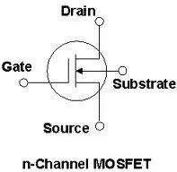
The metal–oxide–semiconductor field-effect transistor (MOSFET, MOS-FET, or MOS FET) is a transistor utilized for amplifying or switching electronic signals. Despite being a four-terminal device with source (S), gate (G), drain (D), and body (B) terminals, in many cases the body (or substrate) of the MOSFET is internally connected to the source terminal. This configuration simplifies the device to a three-terminal form, akin to other field-effect transistors, in electrical diagrams.
The MOSFET is extensively used in both digital and analog circuits, surpassing the once more prevalent bipolar junction transistor (BJT).
In enhancement mode MOSFETs, a voltage applied across the oxide layer induces a conductive channel between the source and drain via the field effect. The term “enhancement mode” signifies the increase in conductivity with an increase in oxide field, which creates carriers in the channel known as the inversion layer. Depending on the type of substrate, the channel can host electrons (nMOSFET or nMOS) or holes (pMOSFET or pMOS), opposite to the substrate type (p-type for nMOS and n-type for pMOS).
In contrast, depletion mode MOSFETs feature a channel with carriers in a surface impurity layer of opposite type to the substrate. Here, conductivity decreases when a field depletes carriers from this surface layer.
symbol:
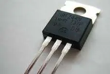
actual photo:
Figure 04: Mosfet
To mitigate the increase in power consumption resulting from gate current leakage, a high-κ dielectric replaces silicon dioxide as the gate insulator, while metal gates replace polysilicon. When a voltage is applied between the gate and body terminals, the electric field penetrates through the oxide layer, creating an “inversion layer” or “channel” at the semiconductor-insulator interface. This inversion channel matches the type (p-type or n-type) of the source and drain, facilitating current flow through it. By adjusting the voltage between the gate and body, the conductivity of this layer is modulated, thereby controlling the current flow between the drain and source. MOSFETs find application in low voltage, low current, and high-frequency scenarios.
Various electrical components used in project
2.3.2 Inductor
Symbol:
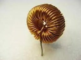
Figure 05: Inductor
An inductor, also known as a coil or reactor, is a passive electrical component with two terminals that opposes changes in electric current passing through it. It typically consists of a conductor, such as wire, wound into a coil. When current flows through an inductor, energy is temporarily stored in a magnetic field within the coil. As the current through the inductor changes, the time-varying magnetic field induces a voltage in the conductor, following Faraday’s law of electromagnetic induction, which opposes the initial change in current.
Inductors act as sources when current tends to decrease, thereby limiting high-peak currents that would otherwise be governed solely by switch resistance. When used to drop voltage, inductors store energy and control the percentage of ripple, influencing whether the circuit operates in continuous mode. The peak current through the inductor determines its required saturation-current rating, which in turn dictates its approximate size.
Saturating the inductor core reduces converter efficiency and increases temperatures of components like the inductor itself, MOSFETs, and diodes. The size of the inductor and capacitor can be minimized by employing high switching frequencies, multi-phase interleaved topologies, and fast hysteretic controllers.
Reducing the value of the inductor enhances transient response speed but increases current ripple, leading to higher conduction losses in switches, inductors, and parasitic resistances. A smaller inductor also necessitates a larger filter capacitor to reduce output voltage ripple.
Inductors used in switched supplies are often wound on toroidal cores made from materials like ferrite or powdered iron, sometimes with distributed air-gaps to store energy. In DC-DC converters, energy is transferred from an input source to an output load at a controlled rate, and as switching frequency rises, the time available for this energy transfer diminishes.
For example, in a buck converter operating at 500 kHz with a 10 µH inductor, increasing the frequency to 1 MHz typically allows the use of half the inductance, or 5 µH, for efficient operation.
2.3.3 Capacitor
Symbol:
Figure 06: Capacitor
A capacitor (originally called a condenser) is a passive electrical component with two terminals used to store energy electrostatically in an electric field. Practical capacitors come in various forms but all consist of at least two electrical conductors (plates) separated by a dielectric (insulator). The conductors can be thin metal films, aluminum foil, or disks, while the dielectric, which does not conduct electricity, enhances the capacitor’s charge capacity. Dielectrics can be made from materials like glass, ceramic, plastic film, air, paper, or mica. Capacitors are essential components in electrical circuits found in many common devices. Unlike resistors, capacitors do not dissipate energy; instead, they store energy in the form of an electrostatic field between their plates.
Capacitors provide filtering by diverting harmonic currents away from the load. In step-down converters, output capacitance across the load minimizes voltage overshoot and ripple. The capacitor must be sufficiently large to maintain a stable voltage during the switch-off period. Inadequate capacitance leads to significant overshoots and voltage ripple, exacerbated by high equivalent-series resistance (ESR) in the capacitor. Design specifications typically dictate maximum allowable output voltage overshoot and ripple, necessitating the use of capacitors with ample capacitance and low ESR to meet these requirements.
Switched power regulators in high-current, high-performance applications require capacitors chosen for minimal losses. Losses in capacitors occur due to internal series resistance and inductance. Solid tantalum capacitors are preferred for their low losses. In some cases, multiple capacitors are paralleled to achieve sufficiently low effective series resistance for very high-performance power supplies.
Follow this link for complete project: BOOST CONVERTER USING ARDUINO

