Today Printed Circuit Boards (PCBs) have become the integral part in many devices that we use in our daily lives. From handheld portable electronic devices, to industrial machines and heavy equipment, communication devices and consumer electronics we see everywhere these PCBs. Today’s PCBs are very complex and different shapes and materials based. They are flex and rigid and have variety of components that are wired together to perform a specific requirement. However this is only possible in the case of multilayer PCBs.
In older times the PCBs were only single or double layer and did only serve the purpose of simple computation or automation while today these PCBs are more advanced and multilayer and flex PCB are commonly found in motherboards, smart phones, smart watches, biomedical instruments, crypto currency mining devices, artificial intelligence based robotic circuits and many more. Also the manufacturing methods have improved in recent past enabling the faster production, cutting down production cost and reducing size of PCBs
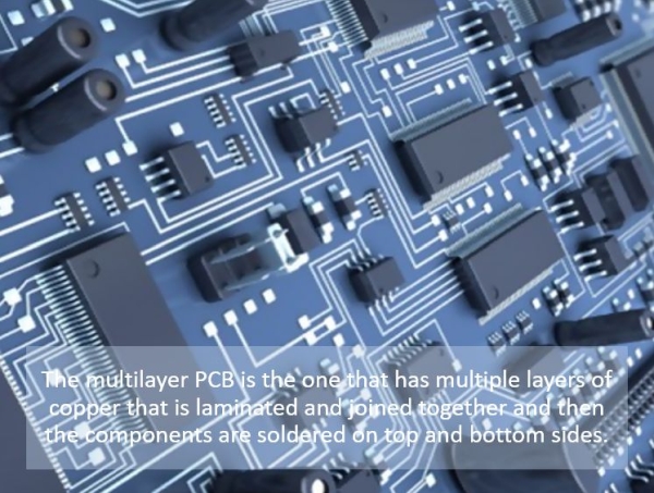
What Is A Multilayer PCB?
The multilayer PCB is the one that has multiple layers of copper that is laminated and joined together and then the components are soldered on top and bottom sides. The inner layers are actually the double sided circuit that are combined with each other to form one thick PCB with multilayers. The components are electrically connected by means of copper tracks and vias and pads/ holes join the interconnections. The vias are of different types like PTH, blind and buried. The result is the complex PCB with maximum circuitry on smaller PCB size.
Why Multilayer PCB Is Needed?
The advent of complex processing and evolving technology, demands the need of PCB layout procedure that can achieve the desired requirements. Also the problems that were occurring in the single or double sided PCBs like noise and stray capacitance was also an issue that caused the invention of multilayer PCB.
How Many Layers For Multilayer PCB:
The multilayer PCBs nowadaysare becoming widespread and available in very small form factor or sizes as compared to single or double sided PCBs. Their thickness also is variable and defendant upon number of layers. Commonly the multilayer PCBs are available from 4 layers to 12 layers depending upon the application and requirements. The layers are usually in even number say 4 layer PCB or 8 layer PCB, the odd numbered layers will cause problems of circuit wrapping and similar type issues. The multilayer PCBs are costly to produce as compared to single sided because of extra steps involved during PCB fabrication but their application are very huge. For example a smart phone can have a PCB with up-to 8 layers and a military electrical equipment can have a PCB with up-to 100 layers. This type of PCB with so many layers are very rare and costly.
Read more: BENEFITS OF MULTILAYER PCB AND APPLICATIONS