Summary of ARDUINO MPPT SOLAR CHARGE CONTROLLER ( Version-3.0)
This article presents a comprehensive tutorial series on building an Arduino-based Solar MPPT (Maximum Power Point Tracking) Charge Controller, version 3.0, designed for 50W solar panels charging 12V lead acid batteries. The project uses an Arduino Nano microcontroller and integrates features like an LCD display, LED indicators, Wi-Fi data logging, USB charging, and multiple protective mechanisms. It includes detailed steps on circuit design, component selection (buck converter, MOSFETs, inductor, capacitors), assembly, testing, and software algorithms for MPPT. Future versions aim to enhance current capacity, voltage ratings, battery management, and expand functionalities.
Parts used in the Arduino Solar MPPT Charge Controller:
- Arduino Nano
- Current Sensor (ACS712-5A)
- Buck Converter (LM2596)
- WiFi Module (ESP8266)
- LCD Display (20x4 I2C)
- MOSFETs (4x IRFZ44N)
- MOSFET Driver (IR2104)
- 3.3V Linear Regulator (AMS1117)
- Transistor (2N2222)
- Diodes (2x IN4148, 1x UF4007)
- TVS Diodes (2x P6KE36CA)
- Resistors (3x 200Ω, 3x 330Ω, 1x 1kΩ, 2x 10kΩ, 2x 20kΩ, 2x 100kΩ, 1x 470kΩ)
- Capacitors (4x 0.1µF, 3x 10µF, 1x 100µF, 1x 220µF)
- Inductor (33µH, 5A)
- LEDs (Red, Yellow, Green)
- Prototype Board
- Wires and Female-Female Jumper Wires
- Header Pins (Male Straight, Female, Right Angle)
- DIP Socket (8 pin)
- Screw Terminals (3x 2-pin, 1x 6-pin)
- Fuses (2x 5A)
- Fuse Holders (2 nos)
- Push Switch (2 nos)
- Rocker/Toggle Switch (1 no)
- Female USB Port (1 no)
- JST Connector (2-pin male-female)
- Heat Sinks
- Enclosure
- Plastic Base and Studs
- Screws, Nuts, Bolts
Greetings to my solar charge controller tutorial series. Two versions of my PWM charge controller have been shared. If you’re new, please check out my previous tutorial to grasp the fundamentals of a charge controller.
1. Version-1
2. Version-2
This tutorial will demonstrate the process of making an Arduino Solar MPPT charge controller that includes an LCD screen, LED lights, data logging via Wi-Fi, and the ability to charge different USB gadgets. It contains various protections to avoid harm in unusual situations.
This controller uses the Arduino Nano microcontroller. This layout is suitable for a 50W solar panel to charge a regularly used 12V lead acid battery. Additional Arduino boards like Pro Mini, Micro, and UNO are also suitable for use.
The most cutting-edge solar charge controller available at present is Maximum Power Point Tracking (MPPT). The MPPT controller is more expensive and complicated, but it provides numerous advantages compared to conventional controllers. It is more efficient in colder temperatures by 30 to 40%, but it is harder to produce than PWM controllers and needs knowledge of power electronics.
I put in a lot of effort to make it easier to comprehend. If you’re already familiar with the fundamentals of MPPT charge controller, you can bypass the initial procedures.
The MPPT circuit is based on a synchronous buck converter circuit that lowers the solar panel’s higher voltage to match the battery’s charging voltage. The Arduino aims to maximize the power output from the solar panel by adjusting the duty cycle to maintain the panel’s peak performance.
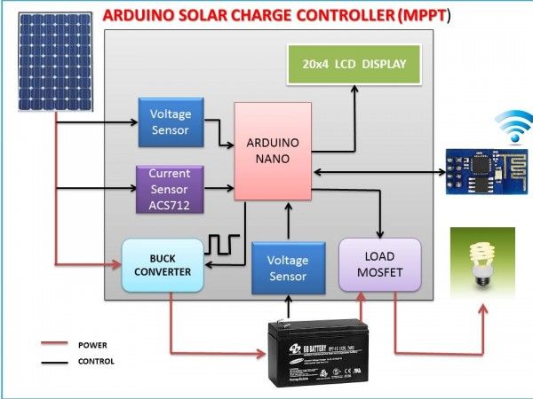
Specification of version-3 charge controller :
1.Based on MPPT algorithm
2. LED indication for the state of charge
3. 20×4 character LCD display for displaying voltages,current,power etc
4. Overvoltage / Lightning protection
5. Reverse power flow protection
6. Short Circuit and Over load protection
7. Wi Fi data logging
8.USB port for Charging Smart Phone /Gadgets
Electrical specifications :
1.Rated Voltage= 12V
2.Maximum current = 5A
3.Maximum load current =10A
4. In put Voltage = Solar panel with Open circuit voltage from 12 to 25V
5.Solar panel power = 50W
This project is consists of 40 steps.So for simplicity I divided the entire project in to small sections.Click on the link which you want to see.
1. Basics on MPPT charge controller
2. Buck circuit working and design calculation
4. Voltage and Current Measurements
5.LCD display and LED indication
8. Making the USB Charging Circuit
10. MPPT algorithm and flow chart
I have spent a lot of time to make this charge controller project.If you like it ,please vote for me in all the competitions.It will be very helpful for me.Thank you in advance.
Step 1: PARTS AND TOOLS REQUIRED:
1. Arduino Nano ( eBay)
2.Current Sensor ( ACS712-5A )
3.Buck Converter ( LM2596 )
4.Wifi Module ( ESP8266 )
5. LCD display ( 20×4 I2C )
6 .MOSFETs ( 4x IRFZ44N )
7. MOSFET driver ( IR2104 )
8. 3.3V Linear regulator ( AMS 1117 )
9. Transistor ( 2N2222 )
10.Diodes ( 2x IN4148 , 1 x UF4007 )
11.TVS diode ( 2x P6KE36CA )
12.Resistors ( 3 x 200R ,3 x330R,1 x 1K, 2 x 10K, 2 x 20K, 2x 100k, 1x 470K )
13.Capacitors ( 4 x 0.1 uF, 3 x 10uF ,1 x100 uF ,1x 220uF)
14.Inductor ( 1x 33uH -5A )
15. LEDs ( 1 x Red ,1 x Yellow ,1 x Green )
16.Prototype Board
17.Wires and Jumper wires ( Female -Female )
18.Header Pins (Male Straight ,female , Right angle )
19. DIP Socket ( 8 pin )
19.Screw Terminals ( 3 x2 pin ,1 x 6pin )
20.Fuses ( 2 x 5A)
21. Fuse Holders (2 nos)
22. Push Switch ( 2 nos)
23.Rocker /Toggle Switch ( 1 no)
24.Female USB port ( 1no)
25. JST connector ( 2pin male -female )
26.Heat Sinks
27.Enclosure
28.Plastic Base and studs
29. Screws/Nuts/Bolts
TOOLS REQUIRED :
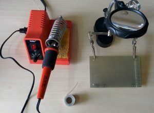
1.Soldering Iron
2. Glue Gun
3. Dremel
4.Hobby Knife
5.Wire Cutter
6.Wire Stripper
7.Screw Driver
8. Ruller and pencil
Step 2: Basics on MPPT charge controller
The voltage output of a solar panel changes depending on several factors like:
Original: “The new restaurant in town has a modern vibe and serves a variety of international cuisines.”
Paraphrased: “The modern-themed new restaurant in the area offers a range of international dishes.” The amount of sunlight. The company’s profits have doubled compared to last year. The load is linked. Rewrite the given text using the same language and ensuring the word count remains the same:
3. Paraphrase the following text using the same input language and keep the same amount of words: The temperature of the solar panel.
Throughout the day and with changing weather conditions, the solar panel will consistently produce varying levels of voltage. For every voltage level, the solar panel will produce a specific current in Amperes. The Amps produced for a certain voltage can be found on the IV curve of a solar panel’s specification sheet, which typically looks similar to the figure-1 displayed above.
The blue line in figure-2 shows a voltage from solar panels of around 30V, paired with a current of about 6.2A. A current of 5A is indicated by a voltage of 35V on the green line.
The relationship between power, voltage, and current is that power is equal to voltage multiplied by current.
In the picture above, while tracing the red curve, you will reach a point where the result of Voltage multiplied by its corresponding Current is greatest compared to any other point on the curve. The solar panel’s Maximum Power Point (MPP) is the term used for this.
What Is MPPT ?
The voltage produced by a solar panel varies according to different factors such as…
1. The level of sunlight 2. The electrical load connected 3. The panel’s temperature.
MPPT is an acronym that stands for Maximum Power Point Tracking. MPPT charge controllers are utilized to maximize power output from PV modules in specific circumstances. To delve deeper into this concept, we must analyze the power curve traits of a solar panel. Refer to the image above, downloaded from the internet, for a visual explanation of MPPT. Thus far, we have observed that the peak power point (MPP) of a solar panel is located at the intersection of the current and voltage curve.
A 12V solar panel may fluctuate between 12V and 21V depending on the connected load and sunlight brightness, due to its internal resistance reacting to varying irradiance levels. Solar panels only operate at their rated power output at a specific voltage and load, which varies with fluctuations in sunlight intensity.
For instance, consider a 100 watt solar panel with a rating of 18V at 5.55 amps.
The Solar panel requires a load of 3.24 ohms, calculated using the 18 V at 5.5 amps rating.
If a different load is connected, the panel will output less than 100 watts. Connecting a static load with a resistance different from the panel’s internal resistance at MPP will result in drawing less power from the panel than its maximum capacity.
Taking a simple example say we connected the above 100W panel directly to a 12V lead acid battery, the panel voltage would be dragged down near to the load voltage of the battery as the batteries resistance is lower than the panels, but the current stays the same at 5.55 amps.This happens because Solar Panels behave like current sources, so the current is determined by the available sunlight.
Now the power (P)= V x I = 12×5.55=66.6W. So the Solar panel is now behaving like a 66 watt panel.
This equates to a loss of 100W-66.6W = 34W ( 33.4%).
This is where MPPT comes into play. MPPT circuits can be based on various switch mode power supply (SMPS) topologies, they generally have a fixed frequency but varying duty cycle. The duty cycle is controlled via an algorithm so as to track the changing MPP.
Step 3: BUCK CONVERTER WORKING
A buck converter is essentially a DC to DC converter. The key principle in a buck converter is the inductor’s resistance to changes in current. The output voltage of a buck converter will never exceed the input voltage. The above image displays a basic diagram of a buck converter.
Working Principle :
When the MOSFET is ON
The inductor (L) has current flowing in a clockwise direction to the load (R) and charges the output capacitor (C) when the mosfets are activated. At this moment, the diode’s cathode has a positive voltage, which puts the diode (D) in reverse bias and stops current from flowing. The current gradually increases as energy is stored in the inductor’s magnetic field, causing a slow start to flow into the load from Vin. Hence, the energy is conserved in the inductor when the mosfet is turned on.
When the MOSFET is OFF
The polarity of the voltage across the inductor changes when the mosfet is switched off. The decline of the inductor’s magnetic field results in the discharge of stored energy, allowing current to flow from the inductor to the load. The diode is currently in forward bias because a negative voltage is connected to the cathode. Therefore, the present flow originating from the inductors releases in a clockwise direction across the load before returning through the diode. Once the inductor loses a certain amount of energy, the load’s voltage decreases, and the capacitor becomes the main source of current, supplying power to the load until the next cycle begins. To continue conduction mode, the inductor must not be fully discharged before the mosfet switches on again, and this cycle is repeated.
What is Synchronous Buck Converter ?
The diode is replaced by another mosfet in synchronous design to improve circuit efficiency by eliminating losses from the diode’s forward voltage drop. Executing this task is a bit trickier because the activation of the second mosfet must be coordinated with the activation of the first mosfet. It is important to make sure that both are not activated at the same time, as this could lead to a direct path to ground, causing a short circuit. The mosfet switching happens in the opposite phase at 180 degrees, separated by a short pause called a Dead-Band.
Step 4: BUCK CONVERTER DESIGN
Designing the buck converter circuit begins with considering the output parameters of the system and its load. The decision was made to target a 12 V output (battery voltage) for a 50W solar panel design.
The frequency of operation, inductor size, and output capacitor size are crucial factors in determining the current and voltage ripple size in a buck circuit calculation. Having minimal current and voltage ripple is preferred.
Typically, smaller inductor and output capacitor sizes result in lower system costs due to higher frequency. On the other hand, increasing PWM frequencies can reduce the effectiveness of the system because of switching losses in the mosfets, requiring a balance that aligns with the end system’s design limitations.
A PWM frequency of 50kHz was selected for this design.
From our previous conversation, we have determined that a buck converter consists of.
1.Inductor
2.Capacitor
3.MOSFETS
In the next few steps I will discuss how to choose these components.
Step 5: INDUCTOR CALCULATION
Determining the inductor value is of utmost importance when designing a buck converter. Firstly, presume that the converter is operating in continuous conduction mode (CCM), as is typically the situation. CCM suggests that the inductor does not completely drain during the off-time of the switch. The next equations are based on a perfect switch (zero resistance when on, infinite resistance when off, and instant switching time) and a perfect diode.
Assume
We are designing for a 50W solar panel and 12V battery
Input voltage (Vin) =15V
Output Voltage (Vout)=12V
Output current (Iout) =50W/12V =4.16A = 4.2A (approx)
Switching Frequency (Fsw)=50 KHz
Duty Cycle (D) =Vout/Vin= 12/15 =0.8 or 80%
Calculation
L= ( Vin-Vout ) x D x 1/Fsw x 1/ dI
Where dI is Ripple current
For a good design typical value of ripple current is in between 30 to 40 % of load current.
Let dI =35% of rated current
dI=35% of 4.2=0.35 x 4.2 =1.47A
So L= (15.0-12.0) x 0.8 x (1/50k) x (1/1.47) = 32.65uH =33uH (approx)
Inductor peak current =Iout+dI/2 = 4.2+(1.47/2) = 4.935A = 5A (approx)
So we have to buy or make a toroid inductor of 33uH and 5A.
You can also use a buck converter design calculator
So 33uH is enough for our design.
Step 6: HOW TO WIND A TOROIDAL INDUCTOR
I gathered several toroidal cores from an old computer power supply. I decided to create an inductor at home using them. Although it was time-consuming, I gained valuable knowledge and had fun in the process. Here are some tips I picked up that will make it easier for you to do the same.
How to Wind the wire :
The first step in creating the buck converter circuit involves examining the system’s output parameters and load. A 12 V output (battery voltage) was chosen for a 50W solar panel design.
I developed a simple tool using a popsicle stick to wind toroidal cores because hand winding is uncomfortable and makes it challenging to achieve tight windings. This device is efficient and enables precise and safe winding. Before creating the inductor, it’s crucial to understand the core’s requirements and the necessary number of turns.
The crucial factors of a toroidal core are
1. Outer diameter(OD)
2.Inner diameter(ID)
3.Height (H)
4.Al value
As I did not know the part number,I used a indirect method to identify it.First I measure the OD and ID of the unknown core by using my vernier caliper,it was around
OD= 23.9mm (.94′”) , ID= 14.2mm(.56″) ,H= 7.9mm( .31″) and yellow white in color.
I used a toroid core chart (page-8) to identify the unknown core.I have attached this toroid size chart in the bellow.It contains a lot of information for the inductor design.The PDF version is attached bellow.
Finding the part number :
I searched the Physical dimension table from the chart. From the table it was found that the core is T94
Finding the mix number :
The color of the core is indication for mix number.As my core is is yellow/white in color,it is confirmed that the mix number is 26
So the unknown core is T94-26
Finding Al value :
From the Al value table for a T94-26 core it is 590 in uH/100 turns.
After selecting the core now time to find out the number of turns required to obtain the desired inductance.
Number of turn (N) = 100 x sqrt( desired inductance in uH / Al in uH per 100 turns)
=> N= 100 sqrt(33/590) = 23.65 = approximately 24 turns
You can also use this online calculator for finding the number of turns.Only you have to know the part number and mix number.
Then I wind a 20 AWG copper wire (24 turns) around the the toroid core.At the both end of the winding leave some extra wire for connection lead.After this remove the enamel insulation from the lead. I used my leatherman file for removing the insulation. See the above picture for better understanding.
Note : Making a good inductor is not so simple.I am still in learning stage.If you are not so confident I will recommend to buy a ready made inductor.
Step 7: CAPACITOR CALCULATION
Output capacitance is necessary in order to reduce the voltage overshoot and ripple found at the output of a buck converter. Insufficient output capacitance leads to significant overshoots, and inadequate capacitance and high equivalent-series resistance (ESR) in the output capacitor result in large voltage ripple. Therefore, in order to adhere to the ripple requirements of a buck converter circuit, you need to have an output capacitor that has sufficient capacitance and low ESR.
Calculation :
The out put capacitor ( Cout)= dI / (8 x Fsw x dV)
Where dV is ripple voltage
Let voltage ripple( dV ) = 20mV
Cout= 1.47/ (8 x 50000 x 0.02 ) = 183.75 uF
By taking some margin, I select 220uF electrolytic capacitor.
The equations used for calculation of inductor and capacitor is taken from a article LC Selection Guide for theDC-DC Synchronous Buck Converter
![]() LC selection.PDF889 KB
LC selection.PDF889 KB
Step 8: MOSFET SELECTION
The vital component of a buck converter is MOSFET.Choosing a right MOSFET from the variety of it available in the market is quite challenging task.
These are few basic parameters for selecting right MOSFET.
1.Voltage Rating : Vds of MOSFET should be greater than 20% or more than the rated voltage.
2.Current Rating: Ids of MOSFET should be greater than 20% or more than the rated current.
3.ON Resistance (Rds on) : Select a MOSFET with low ON Resistance (Ron)
4.Conduction Loss : It depends on Rds(ON) and duty cycle.Keep the conduction loss minimum.
5.Switching Loss: Switching loss occurs during the transition phase.It depends on switching frequency,voltage ,current etc.Try to keep it minimum.
These are few links where you can get more information on selecting the right MOSFET.
1.MOSFET selection for Buck Converter
2.A simple guide to selecting power MOSFETs
In our design the maximum voltage is solar panel open circuit voltage(Voc) which is nearly 21 to 25V and maximum load current is 5A.
I have chosen IRFZ44N MOSFET. The Vds and Ids value have enough margin as well as it has low Rds(On) value.
You can check the other parameters of IRFZ44N from the data sheet
Step 9: MOSFET DRIVER
Why we need a gate driver ?
A Mosfet driver enables a low current digital output signal from a Microcontroller to control the gate of a Mosfet. Using a driver, a high voltage mosfet can be switched by a 5 volt digital signal. The gate capacitance of the MOSFET must be charged in order for it to turn on, and discharged to turn off. The more current provided to the gate, the quicker the switching on/off process, hence the need for a driver.
Fore more details you can read about MOSFET Basics
For this design I am using a IR2104 Half Bridge driver. The IC takes the incoming PWM signal from the micro controller, and then drives two outputs for a High and a Low Side MOSFET.
How to use it ?
From the data sheet I have taken the image shown above.
Input :
First we have to provide power to the gate driver.It is give on Vcc (pin-1) and its value is in between 10-20V as per data sheet.
The high frequency PWM signal from Arduino goes to IN (pin-2) . The shut down control signal from the Arduino is connected on SD ( pin 3).
Output :
The 2 output PWM signals are generated from HI and LO pin. This gives the user the opportunity to fine tune the dead-band switching of the MOSFETs.
Charge Pump Circuit :
The capacitor connected between VB and VS along with the diode form the charge pump.This circuit doubles the input voltage so the high switch can be driven on. However this bootstrap circuit only works when the MOSFETs are switching.
The data sheet of IR2104 is attached here
![]() IR2104 data sheet.pdf137 KB
IR2104 data sheet.pdf137 KB
Step 10: SCHEMATIC AND WORKING
The screw terminals JP1 and JP2 are utilized for linking the solar panels to the power input and battery output, in that order. JP3, the third terminal, is designated for the connection of the load.
The safety fuses F1 and F2 have a rating of 5A.
The buck converter is made up of the synchronous MOSFET switches Q2 and Q3, inductor L1, and capacitors C1 and C2. The inductor and capacitor C2 aid in smoothing out the switching current and the output voltage. Capacitor C8 and resistor R6 work together to create a snubber network, which helps decrease the inductor voltage ringing caused by the switching current.
In my old charge controller, a diode was used to block battery power from flowing back into the solar panels at night, but now a third MOSFET Q1 has been added for the same function. Because diodes exhibit a voltage drop, a MOSFET is much more effective. Q1 is triggered by the passage of voltage through D1 which results in the activation of Q2. When Q2 deactivates, R1 releases the voltage from Q1’s gate resulting in its deactivation.
Diode D3 (UF4007) is a fast diode that starts conducting electricity before Q3 is activated. The objective is to improve the effectiveness of the converter.
The IC IR2104 serves as a gate driver for a half bridge MOSFET. The IR2104 is employed to regulate the high and low side MOSFETs using the PWM signal from the arduino (Pin -D9). The Arduino on pin 3 can also disable it with a control signal (low on pin -D8). D2 and C7 form part of the bootstrap circuit that generates the high side gate drive voltage for Q1 and Q2. The program watches over the PWM duty cycle to prevent it from reaching 100% or staying on constantly. It constrains the PWM duty cycle to 99.9% to maintain functioning of the charge pump.
Two voltage divider circuits, consisting of R1 and R2 for measuring solar panel voltage and R3 and R4 for measuring battery voltage, are employed. The voltage signal is sent to Analog pin-0 and Analog pin-2 by the dividers. Ceramic capacitors C3 and C4 aid in the removal of high frequency spikes.
Mosfet Q4 is used for regulating the load. The driver consists of a transistor along with resistors R9, R10.
Diodes D4 and D5 act as transient voltage suppression (TVS) diodes to safeguard against overvoltage originating from both the solar panel and the load side.
The current sensor ACS712 identifies the current from the solar panel and transmits it to analog pin-1 on the Arduino.
The microcontroller’s digital pins are linked to the 3 LEDs, serving as an output interface to show the charging status.
The reset button comes in handy when the code becomes unresponsive.
The purpose of the back light switch is to manage the back light of the LCD display.
.
Step 11: Test the gate driver and MOSFETs Switching
Hey, I believe I have covered the theory extensively. Let’s switch to practical experiments now.
Like I mentioned before, the Buck Converter is the core of the MPPT charge controller. If the buck converter circuit functions properly, everything else will be much easier. Let’s start by testing the Mosfets switching and the driver.
I always ask to solder on a breadboard before proceeding. I have accidentally blown many MOSFETs while testing, so please be cautious with the connections.
Connect all components according to the provided schematic. TVS diode, current sensor, and voltage divider can be excluded.
After plugging in all components, measure the resistance across the input rail. It should show a reading of multiple kiloOhms. If the resistance measures below 1K, revisit the circuit’s connections.
Attach the text file with the code and upload it to the Arduino for testing the sketch.
Next, establish the connection of the scope between the Q1 source and GND.
The outcome needs to be a PWM signal traveling at a rate of 50KHz.
The waveforms gathered during my experiments are displayed up there.
If everything goes according to plan, continue with the assembly of the bulk converter circuit by adding the inductor and capacitor.
![]() test_code.txt843 bytes
test_code.txt843 bytes
Step 12: Test the Buck Converter
After determining the ratings for the inductor and capacitor in previous steps, we are now ready to utilize and test them.
Install the 33uH inductor and 100uF input and 220uF output electrolytic capacitor according to the diagram. Additionally, you may include 0.1uF ceramic capacitors alongside the input and output capacitors for improved performance. However, this step is optional.
Next, create the snubber circuit with a 0.1uF ceramic capacitor and a 200ohm resistor.
Once more, test the resistance between the input rail. It should be in the range of kiloohms.
Now provide the input rail and Arduino with power.
Attach the scope’s probe between the output capacitor.
The outcome is displayed above. The output must be a consistent direct current.
Vout equals the product of Duty Cycle and Vin.
When a 12V input supply is given a 50% duty cycle, the output on the scope should read 6V.
Once it has been verified that everything is functioning properly, we can now install the blocking mosfet Q1. This component is utilized to prevent reverse power flow from the battery to the solar panel at night.
Insert the third mosfet Q3 in accordance with the diagram. Next, position the 470k resistor and IN4148 diode.
Make sure to review the output once more to ensure it remains identical.
Finally, place the scope between the Q1 gate and Gnd.
Are you aware that you have completed the most crucial aspect of this project?
Step 13: VOLTAGE MEASUREMENT
Voltage Measurement :
Arduino’s analog inputs can detect 0-5V DC voltage using a 5V analog reference, which can be extended with a voltage divider consisting of two resistors. The voltage divider decreases the voltage to a level appropriate for the Arduino analog inputs. This can be used to measure the voltages of the solar panel and battery.
For a voltage divider circuit
Vout = R2/(R1+R2) x Vin
Vin = (R1+R2)/R2 x Vout
The analogRead() function reads the voltage and converts it to a number between 0 and 1023
Example code :
// read the input on analog pin 0 ( You can use any pin from A0 to A5)
int Value = analogRead(A0);
Serial.println(value);
The bove code gives an ADC value in between 0 to 1023
Calibration :
We’re going to read output value with one of the analog inputs of Arduino and its analogRead() function. That function outputs a value between 0 (0V in input) and 1023 (5V in input)
that is 0,0049V for each increment (As 5/1024 = 0.0049V)
Vin = Vout*(R1+R2)/R2 ; R1=100k and R2=20k
Vin= ADC count*0.0049*(120/20) Volt // Highlighted part is Scale factor
Note : This leads us to believe that a reading of 1023 corresponds to an input voltage of exactly 5.000 volts.
In practical you may not get 5V always from the arduino pin 5V .So during calibration first measure the voltage between the 5v and GND pins of arduino by using a multimeter,and use
1ADC = measured voltage/1024 instead of 5/1024
Check your voltage sensor by a test code attached bellow
Step 14: CURRENT MEASUREMENT
For current measurement I used a Hall Effect current sensor ACS 712 (5A).
The ACS712 sensor read the current value and convert it into a relevant voltage value, The value that links the two measurements is sensitivity.You can find it on the datasheet.
As per data sheet for a ACS 712 (5A) model :
1. Sensitivity is 185mV/A.
2. The sensor can measure positive and negative currents (range -5A…5A),
3. Power supply is 5V
4. Middle sensing voltage is 2.5V when no current.
Calibration:
Value = (5/1024)*analog read value
// If you are not getting 5V from arduino 5V pin then, value = ( Vmeasured/1024 ) * analog read value
// Vmeasured is the voltage in between Arduino pin 5V and GND. You can measure it by a multimeter.
But as per data sheets offset is 2.5V (When current zero you will get 2.5V from the sensor’s output)
Current in amp = (value-2.5)/0.185
Test it by a sample code for ACS712 attached bellow.
Step 15: LCD Display and LED Indication
LCD display :
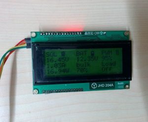
A 20-character by 4-line LCD is used for monitoring the solar panel, battery, and load parameters. We have chosen an I2C LCD display for simplicity. Just 4 wires are needed to establish a connection with the Arduino. In an earlier iteration, the LCD screen was consuming a considerable amount of energy. The main factor was the LCD backlight. I choose to put in a push button in order to control the backlight. The default setting will turn off the backlight. Pressing the switch will activate it for 15 seconds before shutting off.
Vcc–> 5V , GND–>GND, SDA–>A4 and SCL–>A5
Column-1: Solar panel voltage, Current and Power
Column-2: Battery Voltage, Charger state, and SOC
column-3: PWM duty cycle and load status
For testing the LCD download the test code attached bellow.
You download the library from LiquidCrystal_I2C .
LED indication :
Red, Green and Yellow LEDs are used to indicate the battery voltage level.
Low Voltage — > Red led
Normal Voltage –> Green Led
Fully Charged –> Yellow Led
Step 16: HARDWARE AND SOLDERING
Before soldering you should clear about the Power and Control Signal. Do not mix up between them. Otherwise, you will fry everything.
Power Signal :
1.Solar panel -> Fuse -> Current sensor -> Mosfets Q1,Q2 ,Q3 -> Inductor -> Battery.
2.Battery -> Fuse -> Load -> Mosfet Q4
Control Signals :
1.The signal from the different Sensors to Arduino
2. Signals from the Arduino to the Mosfet drivers, LED and LCD
3. The signal between the Arduino and ESP8266
I used red and black thick wires ( 0.5 to 0.75 sq mm) for power and ground connections respectively.
All the colored thin wires are for control signals.
Tips: Print the PDF format Schematics before soldering. Keep it in front of you during soldering for reference.
Step 17: Drill Holes for Mounting
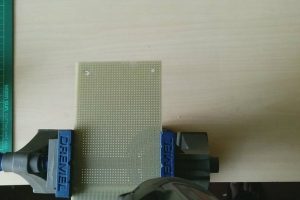
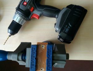
First, hold the prototype board by a vice.
Then drill 4 holes (3mm) at the 4 corners of the prototype board.
Step 18: Add the Input and Out Put Terminals :
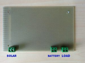
First solder the three screw terminals for solar panel, battery and load connection.
The left one is for solar panel, the middle one is for battery and the right one is for load connection.
Step 19: Add the Fuse Holders
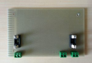
On the extreme left and right solder the two fuse holders.( One in the solar panel side and other on the load side)
Then connect the left terminal of the solar screw terminal with one leg of the fuse holder.
Step 20: Solder the MOSFETS and Input Capacitor
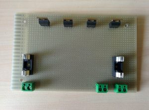
Place all 4 MOSFETs evenly spaced on the top of the prototype board and ensure there is enough room for attaching heat sinks.
Next, include a 100uF capacitor in the circuit. I created extra room between the fuse holder and capacitor for future installation of the current sensor.
Connect wires with solder in the following manner:
Between the positive end of the input capacitor (C) and the gate of the mosfet Q1.
Between drains of mosfet Q1 and Q2.
Then in between source of Q2 and drain of Q3.
Step 21: Mounting the Arduino Nano
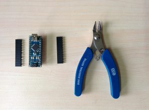
Start by cutting two rows of female and male header pins, each with 15 pins. I utilized a diagonal nipper for cutting the headers.
Next, attach the male header pins. Ensure that the spacing between the two rails is suitable for the Arduino Nano.
Keep a space of two rows next to the female header before soldering the two male headers.
After that, connect the matching male and female pins. I overlooked this step while soldering.
Female headers are utilized to attach the Arduino nano while male headers connect externally to the Arduino.
Step 22: Make the Power Supply
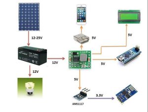
Energy is needed to run the Arduino, as well as different sensors, LED, LCD, and the wifi module (ESP8266).
Every module can function with a 5V power source, except for the ESP8266 module, which needs a maximum of 3.7V. Operating it at a voltage of 3.3V is recommended. Despite having a 3.3V pin, the Arduino Nano cannot provide sufficient power (around 200mA to 300mA) for the ESP8266 module. Hence, it is necessary to have an independent 3.3V power supply that can provide a minimum of 300mA.
5V Power Supply :
I previously utilized a LM7805 linear voltage regulator to reduce the battery voltage to 5V for the power supply, but it generated excess heat. Therefore, I opted for a highly efficient buck converter in this iteration.
Modify the output voltage of the buck converter.
Initially, attach the battery to the input terminal of the buck converter and then fine-tune the potentiometer to achieve an output of 5 volts.
Look at the picture above.
Get ready 4 male headers with 2 pins each and solder them to the designated holes in the converter.
Place the converter on top of the four header pins and secure it by soldering. Make sure the side with the input is towards the battery screw terminal.
Position capacitor C2 near the terminal of the battery screw. Make sure the left side of the capacitor is where the positive terminal is located.
Then, connect the input of the buck converter to the battery screw terminal and the output to the 5V and GND pins of the Arduino Nano. Confirm the configuration by positioning the Arduino Nano on the header pin and linking the 12V battery to the screw terminal. If performed accurately, the Arduino power LED will light up.
Lastly, attach two rows of male header pins on the edge of the Arduino 5V and GND pins to allow for external connections.
3.3V Power Supply :
I am planning to use a voltage regulator AMS1117 to step down from 5V to 3.3V.
Solder the voltage regulator first, then add two 10uF capacitors. One on the input and other on the output side.
See the above schematic.
Step 23: Solder the Mosfet Driver Circuit
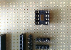
First solder the 8 pins DIP socket just above the arduino header pins.
Add 10uF capacitor and and a 0.1uF capacitor in between the pin-1 and pin-4.
Solder the diode (D2) in between pin -1 and 8.The diode cathode should be connect to the pin-8.
Solder the capacitor (C7) in between pin-8 and pin-6.
Solder two 200ohm resistors ( R7 and R8) just side to the pin-2 and pin-3.
Solder one 470K resistor (R1) near to the mosfet Q1 and a diode (D1) in between gates of mosfets Q1 and Q2.The diode cathode connects to the gate of Q1.
After this complete the circuit by soldering wires as per the schematics.
Step 24: Solder the Voltage Sensors
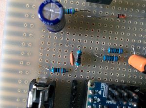
Solder solar panel voltage divider near to the fuse and battery voltage divider near to the output capacitor.
Then solder two ceramic capacitors ( C3 and C4) across the 20k resitors.
Then solder a wire between middle point of the solar panel side voltage divider and arduino pin A0.
Finally solder a wire between middle point of the battery side voltage divider and arduino pin A2.
Step 25: Solder the Inductor and Snubber Circuit
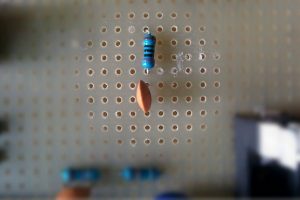
First solder the resistor (R6) and capacitor ( C8) in series just above the output capacitor( C2).
Then solder the inductor parallel to it.
Inductor is the heavier component in the entire circuit.To sit it firmly, apply glue at the base.
Then solder the ultra fast diode (D3) .
Step 26: Solder the Load Mosfet (Q4) Driver
Solder the 2N2222 transistor near the gate of the mosfet (Q4).
Then add a 10k resistor (R9) near to the collector and a 1k resistor( R10) near to the base.
Then connect the points as per schematic.
Step 27: Adding the Current Sensor
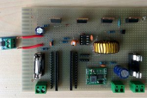
Solder two thick wire in between the solar panel side fuse and capacitor (C1).
Then screw the wire in to the ACS712 screw terminal.
Step 28: Solder the TVS Diodes
I do not have spare TVS diode.So I solder it later.You can solder it earlier also.
One TVS diodes, D4 near the connector JP1 and D5 near the connector JP3.
Note : I am using bidirectional TVS diode.So no polarity mark is there.
Step 29: Connect the GND
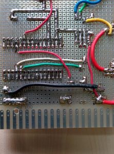
After soldering all the components, connect all the grounds (GND) shown in the schematic.
I am using thick black wires.
Step 30: Make the USB Charging Circuit
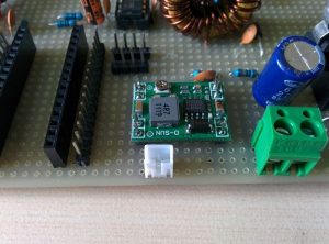
The buck converter used for power supply can deliver maximum current 3A. So the power supply have sufficient margin for charging the USB gadgets.
Make the Circuit :
Solder the male JST connector close to the buck converter and connect two pins together with positive (5V) and negative.
(Ground) comes out of the converter. Look at the picture.
Insert the USB port and switch into their assigned openings, then secure them in place with hot glue.
Connect the positive red wire from the JST connector to one switch terminal, then link a small red wire from another switch terminal to the USB Vcc terminal. Finally, attach the JST connector’s black negative wire to the USB GND.
Check the diagram for the layout of USB pins.
You are also able to take this step beforehand.
Step 31: Make the Wifi Module ( ESP8266 ) Circuit
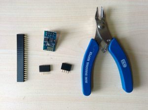
Start by cutting two female headers, each with four pins.
The solder is positioned next to the fuse holder on the side where the load is connected.
Use the diagram to complete the circuit.
Be careful when soldering this part. This module will be damaged if the voltage goes above 3.7 V because it operates at 3.3 V.
I plan to utilize a 3.3 V regulator (AMS1117) to deliver power to this module, making sure the voltage stays within the specified limit for the serial lines. A voltage divider circuit is used to lower the 5V transmit voltage of the Arduino to match the 3.3V receive voltage of the ESP8266.
Setting up the ESP8266 :
The first thing you want to do with ESP8266 is to establish communication.You can see this example project for setting up the ESP8266.Then connect it to your WiFi router.
Hey now you are ready to upload your data to the web.
You can see the following projects to get some idea to use ESP8266 for data uploading to web.
https://www.instructables.com/id/ESP8266-Wifi-Tempe…
http://www.element14.com/community/groups/internet…
The ESP8266 connection schematic is taken from http://www.martyncurrey.com
Step 32: WiFi Data Logging and Scientific Exploration
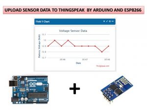
As the solar panel are installed at remote location,monitoring systems parameter is vital for us.This gives me the idea to add the data logging feature to my controller.
The WiFi module( ESP8266 ) automatically uploads live power generation, voltage,Current data to the Web( https://thingspeak.com/ ).Then the web application graph and tabulate data in live.You can download the feeds from the website in the form of a Xcel sheet.Then explore these data for further analysis.I attached a sample of feeds downloaded from thingspeak.
The test code is attached bellow.Hey if you are really excited to see how the tiny WiFi module upload data to the web.Just upload the test code attached bellow.You can test it without any sensor hook to the arduino.Though you will get arbitrary values.It is just for fun 🙂
See the graphs on thingspeak.com .Interesting ??
Note : You can use this test code for other multi sensor system like: weather station .Just you have to calibrate your sensors accordingly.
Go to Data Import/Export and then click on Download.See the above pics.
If you are app developer,then develop a apps for Android, iPhone and Windows Mobile to see these useful data.If you make please share me.I am not a developer.
Step 33: Make the LED Panel
Take a small size rectangular prototype board and drill holes at both end for mounting on the enclosure.
Solder the Leds with equally spaced.
Then solder the 330 ohm resistors (R11,R12 and R13) and 4pin male headers.
Finally complete the circuit as per schematics.
Step 34: Make the Back Light and Reset Switch
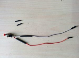
Take 5 female -female jumper wires and cut one side headers in all.
Insert heat shrink tube in all jumper wires.
Reset Switch :
Solder two jumper wires directly to the two pin of the push switch.
Back Light Switch :
Solder two jumper wires to the two pins of the switch.
Solder a 10k resistor to any one pin of the switch.
Then solder a jumper wire to the other end of the resistor.
Finally cover the joints with heat shrink tube and apply hot air.
Step 35: Prepare the Enclosure
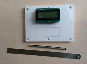
I used a 6″ x 8″ plastic enclosure.
Identify the sizes of the LCD, USB, and Switch. Next, using a Dremel, trim out the rectangular section. Complete the edges by using a hobby knife at the end.
Next, use a pencil to indicate the location of the mounting holes for the LCD, LED panel, switches, and external screw terminal.
Make holes at every designated spot.
Please take note that the holes for LEDs are 5mm in size, switches are 7mm, and all others are 3mm.
Step 36: Make the External Connection Terminal
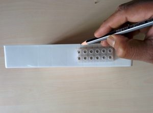
The external connector is used for outside access of all the 3 screw terminals in the controller board.
Mark the hole positions for mounting and 6 wires.
Then screw the wires in all the terminals.Use different color to distinguish between positive and negative terminal.
Step 37: Mount Everything
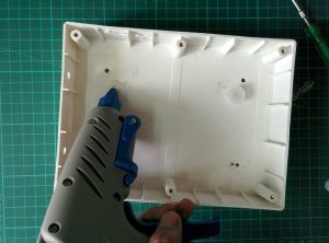
To mount the controller board I used 4 plastic bases.Screw the main board over the base.
Mount the LCD and Led panel by screw and bolts.
Then mount the two switches.
Step 38: Connect All the Panel and Switches
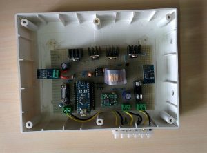
After mounting everything connect the panels,switches and external connector.
Use female-female jumper wires for connecting the panels.
Refer schematics for connection.
Finally box up the enclosure.
Step 39: Software and Algorithm
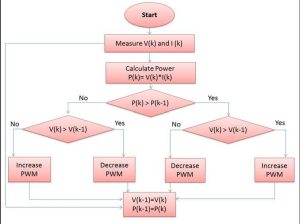
The Maximum Power Tracker utilizes an iterative approach to find the ever-changing Maximum Power Point (MPP). The Perturb and Observe technique, also referred to as the hill climbing algorithm, is employed for Maximum Power Point Tracking. The controller adjusts the voltage a little bit coming from the solar panel and examines the power. When power rises, further adjustments are made in that direction until power levels off.
In the beginning, the voltage to the solar panel is increased; if the output power increases, the voltage is further increased until the output power starts to decline. When the output power decreases, the voltage to the solar panel will decrease until it reaches its maximum power. This process will continue until Maximum Power Point Tracking is reached. This result is a variation in the power output at the peak power point.
Get all the software that is downloadable from my GitHub page.
Step 40: Version-4 Design Ideas and Planning
I want to express gratitude to the new project members Keth Hungerford and Petar for their active involvement. Keith is taking on the main role in designing the new version of the Charge controller.
We currently intend to implement the following modifications in the current version of the charge controller.
Changes at the moment are:
1.Increase panel voltage rating to allow for panels with 60 cells (i.e up to 40 V, so-called “grid connect” panels);
2.Higher current rating, at least 20 amps and preferably 40 amps;
3.Metering current on the battery and load;
4.Improve design robustness to ensure external conditions do not cause any failures;
5. Design that allows multiple controllers to feed into a power distribution switchboard;
6. Optimal battery management for several different battery types, such as Lead Acid (several variants), NiFe, LiFePO;
7. Ability to control more than one load output – either to allow for greater capacity, or timing control of when the output is on or off.
8.Real time clock with date to enable time stamping of statistics and timer control of loads.
9.Operational configuration capability (buttons or via WiFi?);
10.Greater data collection to get illumination statistics, battery performance statistics, load statistics.
11.Higher battery voltage (to 24 or 48 V) and associated higher solar panel voltages;
12.Much higher panel voltage (to 150 V or so)
13.Multiple Load outputs regulated to close to 12 V
14.Panel safety and overload disconnect
In addition there are some “internal” matters that are worthy of investigation:
- Focus on maximising efficiency
- Fail-safe software or self-recovery features
- MPPT algorithm refinements
- will it all fit in Arduino Nano? or selecting another Arduino Board ?
All the ongoing activities are given in Arduino-MPPT-V4 folder ( .rar file).
I request to all of my followers,team members and viewers to give suggestions on it.
You can write your suggestions/feedback in the comment section below.
Step 41: Overview of Version-3.1
After lot testing we observed that MOSFET ( Q3 ) in ver-3.0 design is burning repeatedly.We tried to modify the existing software but not find any satisfactory result.
The other problem was that MOSFET Q1 ( in V-3.0) conduct even when there is no solar input. To solve the above problems and enhance the power handling capability we are modifying both the hardware and software.This is named as Version-3.1 Charge Controller.
This version is not completed yet.So wait until it is complete.
Don’t worry we are making a solution for those who have made the V-3.0 prototype.After little modification we will able to use the new software.
You can see the updates on Hackaday.com
This version have 3 options.
1. 5 Amp version :
A T94-26 toroidal core requires 48 turns of AWG20 wire in order to achieve an inductance of 135 uH, which corresponds to almost 1.5 meters of wire.
Three sets of IRFZ44N MOSFET pairs (totaling 6 MOSFETs) include Q1, Q2, and Q3.
C1 will consist of three 220 uF low ESR capacitors connected in parallel, while C2 will be a singular 220 uF low ESR capacitor.
One ACS712 alone on the panel side according to version 3.0.
2. 8 Amp version :
T106-26 toroid wound with 23 turns of a compound wire made from 3 strands of AWG20 wire twisted together to give 47 uH (this takes about 3.1 m of wire).
Q2 will be a pair of FDP150N10A MOSFETs in parallel.
C1 will be 5 * 220 uF low ESR capacitors in parallel,C2 will be a single 220 uF low ESR capacitor
Two ACS712, one on the panel side as per version 3.0 and one in series with the battery.
3 10 Amp version :
T130-26 toroid wound with 23 turns of a compound wire made from 4 strands of AWG18 wire twisted together to give 41 uH (this takes about 4.5 m of wire).
Q2 will be a pair of FDP150N10A MOSFETs in parallel.
C1 will be 6 * 220 uF low ESR capacitors in parallel,C2 will be 2 * 220 uF low ESR capacitors in parallel.
Three ACS712, one on the panel side as per version 3.0, one in series with the battery and one in series with the load.
The drive circuitry (common to all 3 versions) will use 3 separate IR2104 driver chips, one for each of Q1, Q2 and Q3. We drive the Q1 and Q2 drivers from pin D9 and HO1 and HO2, and drive Q3 from pin D10 and LO3.
In driver chips 1 and 2, pins IN and SD are driven in parallel by Arduino output pin D9. In the case of driver 1 (for Q1) there is a low pass RC filter in series, with a time constant of about 1 ms. Driver 2 is driven directly (as in the current circuit, but probably with a slightly higher series resistor to allow more current for the Q1 driver and its RC filter).
In driver chip 3, IN is driven by D9 and SD is driven by D10.
Separate drivers for Q2 and Q3 are used so that we can turn OFF Q3 to function in Asynchronous mode at low current levels when the controller is in DCM (Discontinuous Current Mode). There might be a more efficient solution, but for the limited time we have, this straightforward option is quick, easy, and dependable to execute.
Each of the 3 models will come equipped with LCD screens, WiFi capabilities, and LED lights (potentially with a more elaborate system to differentiate between DCM and CCM).
Each of the three variations must be capable of handling panels rated at either 18 V or 30 V, and they are equipped with algorithms that prevent damage in case the panel generates excessive current beyond its rating. All of this can be automatically detected.
Every part that comes into contact with panel voltage must have a rating of at least 40 V, especially C1 and our buck converter which provides 12V for the drivers and control electronics.
Step 42: Conclusion
I have put in my utmost effort to create this instructable. I am still expanding my knowledge on MPPT. If I have made any errors, please forgive me and leave a comment. I will fix it promptly.
I enjoy receiving comments on my work! The previous iteration of charge controllers has garnered extensive feedback, with numerous users sharing images of their configuration.
Please share pictures and videos if you create your own controller following this Instructable.
Finally, I want to express my gratitude to timnolan. I have acquired knowledge and applied various elements from his design.
