Summary of Arduino DC-DC Boost Converter Design Circuit with Control Loop
This article explains designing a 10W boost converter controlled by an Arduino Uno. The discrete boost converter uses an inductor, diode, capacitor, and FET to step up voltages efficiently while operating in continuous conduction mode to prevent output voltage drops and electromagnetic interference. Simulations in LTspice validate the design, with practical tests showing up to 100V output and around 90% efficiency at certain voltages. Arduino code uses PWM (62kHz) for control, leveraging a PID loop with feedback via a resistor divider. Proper component ratings and current limiting ensure safe operation.
Parts used in the Arduino DC-DC Boost Converter Design Circuit:
- Inductor 330µH 2.8A (Digikey 811-1335-ND)
- MOSFET N-Channel IRLI640GPBF (Digikey IRLI640GPBF-ND)
- Schottky Diode 150V 3A (Digikey 497-3216-1-ND)
- Aluminum Capacitor 47µF 160V (Digikey 493-1164-ND)
- Resistor 150Ω 5W (Digikey 150W-5-ND)
- Arduino Uno (for PWM control)
- Resistor feedback network: 1KΩ and 100KΩ resistors
This article will discuss the process of utilizing an Arduino Uno to effectively manage a boost converter with a power output of at least 10 watts.
By utilizing only a few components such as an inductor, capacitor, diode, and a FET, it is possible to create a discrete boost converter. Please refer to the Wikipedia page to understand how the circuit functions. The idea is based on the concept that an inductor can store energy in its magnetic field, and when the magnetic field collapses (switch opens), it will oppose the change in current and switch its magnetic field direction to maintain current flow. The voltage at the switch node can be calculated by adding up the voltages from input to output, resulting in a higher voltage at the output.
Keeping the switch closed 100% of the time will merely charge the inductor and the output will equal 0V. Keeping the switch open 100% of the time will cause the inductor to act as a resistor at steady-state and the output will approximately equal the input voltage. Turning the switch OFF and ON rapidly will allow the inductor to charge itself when the switch is closed and then dump energy into the output capacitor when the switch is opened. Care must be taken into choosing how long to keep the switch closed since you do not want to saturate the inductor and cause the current to drop to 0A. The two different modes of operation, continues and discontinuous, refer to the current through the inductor. See this paper for more information on the two modes. Essentially you will want your circuit to operate in continues mode so that the the output voltage does not droop below the intended target and it lessen the effect on radiated emissions which will need to be mitaged to pass CE certification.
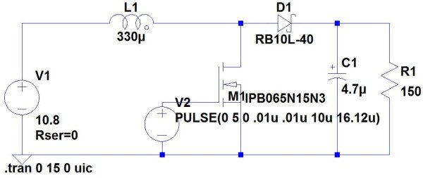
Here is the circuit I made in LTspice, a popular and free SPICE simulation software. Another option is to use the Lite version OrCAD PSpice Designer. I’ve used both and the OrCAD one seems less clunky than the LTspice version.
| RefDes | Digkey | Description | |
|---|---|---|---|
| L1 | 811-1335-ND | IND 330UH 2.8A 150 MOHM | |
| Q1 | IRLI640GPBF-ND | MOSFET N-CH 200V 9.9A TO220FP | |
| D1 | 497-3216-1-ND | DIODE SCHOTTKY 150V 3A | |
| C1 | 493-1164-ND | CAP ALUM 47UF 20% 160V RADIAL | |
| R1 | 150W-5-ND | RES 150 OHM 5W 5% AXIAL |
This boost converter is capable of increasing a low voltage, like a few volts, to a higher voltage of over 100V as long as the maximum limits of the components mentioned are not exceeded. The efficiency of the converter is highest when the difference between output and input voltage is minimal. Increasing a 5V input to 80V will not have the same efficiency as increasing from 40V to 80V. You’ll have to test the simulation to find the output versus input curve without overloading the inductor. This design can achieve a boost from 5V to 100V under high loads, however, it will draw excessive input current under lower loads.
For safety reasons, make sure to acquire a power supply that can limit the current to 2.5A. This will guarantee the protection of the inductor and schottky diode from any harm. The output voltage should stay below ~140V as the schottky’s blocking voltage is up to 150V and the capacitor’s rating is 160V.
Simulation
Prior to buying the aforementioned components, I conducted basic simulations in LTspice. The input current must not exceed 2A while ensuring the output voltage falls within the range of 24V to 100V. The FET is fed a square wave signal to mimic the Arduino PWM. I adjusted it to 62KHz, the maximum PWM frequency of the Arduino. The timing was modified to reach different voltage levels and to function in continuous conduction mode (current doesn’t drop to zero).
10V Input to 24V Output

4.8V Input to 11V Output

Notice how these two images show a different output voltage, yet the same PWM period. The real-life PID should correct the PWM output to produce a constant 24V output.
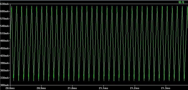
Below shows the inductor current varying between .6A and .3A. This is what we want.
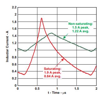
This picture from this TI app note shows a discontinuous current mode. Notice how the current drops to 0 before the switch is closed again.
‘
Lab Data
Here is a table of efficiencies across different input and output voltages
| Input (V) | Input Current (A) | Input Power (W) | Output (V) | Output Current (A) | Output Resistance (Ohm) | Output Power (W) | Eff (%) | Setpoint (ADC) | PWM (counts) |
|---|---|---|---|---|---|---|---|---|---|
| 4V | 1.35A | 5.4W | 24.97V | 0.164A | 152Ohm | 4.1W | 76% | 46 | 219 |
| 5.3V | 0.87A | 4.611W | 24.58V | 0.167A | 152Ohm | 4.04W | 86% | 46 | 210 |
| 10.6V | 0.37A | 3.922W | 24.23V | 0.159A | 152Ohm | 3.86W | 98% | 46 | 142 |
| 15.7V | 0.255A | 4.0W | 24.5V | 0.161A | 152Ohm | 3.949W | 99% | 46 | 78 |
| 10.3V | 1.45A | 14.93W | 45.4V | 0.2986A | 152Ohm | 13.56W | 91% | 92 | 198 |
| 15.7V | 0.91A | 14.28W | 45.4V | 0.296A | 152Ohm | 13.45W | 94% | 92 | 167 |
| 15.7V | 0.08A | 1.256W | 99V | 0.0099A | ~10000Ohm | .9801W | 78% | 200 | 91 |
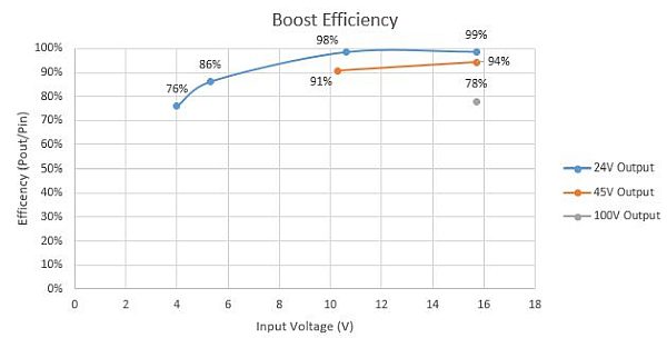
You should notice a few trends.
- The Arduino PWM value is on LESS as the efficiency increases.
- The efficiency goes up as the difference between output to input voltage decreases
- Input current goes up as the efficiency goes down
During testing, the 150 Ohm 5W resistor will become hot. You can sense the warmth emanating from the parcel. It has been demonstrated that 100V is achievable, however the current output reached only 10mA. I could raise this amount to a significant level, but I lacked a resistor that wouldn’t get burned. This can be easily modified to function with nixie tubes.
I attempted to increase a 3.3V output to 24V, however the 300uH inductor reached its saturation point and limited the output voltage to 18V. If you observe this occurring in your control circuit, I suggest increasing the value of your inductor.
Arduino Code
github of the Arduino source code.
The code uses PWM pin 6 to control the FET and a resistor feedback network on pin 0.
The feedback network consists of a 1K resistor to GND and 100K between the ADC pin and the output voltage. The ADC value can be determined as follows: ADC = Vout * 1k/(100k+1k) ===> ADC = Vout*1/101 So, a 10V output will read 99mV on the arduino pin. The arduino pin should never exceed 5V. It is 10-bits, so each bit resembles ~4.8mV (5V/1023). A 24V output would yield an ADC reading of 48 (24V/101) / (5/1023). You can improve the resolution by using say 1K and 10K resistor network. I only had a 100K resistor laying around.
I am using this PID library. The PID constants were chosen based on experimentation. The trick is to 0 your Ki and Kd and play around with Kp until the system oscillates. You should see the input current bounce up and down around the set-point. Then increase Ki a bit until the settling offset error is eliminated. Increase Kd to mitigate the high dv/dt spikes. double Kp=.2, Ki=.4, Kd=0;
I had to adjust the PWM frequency to 62KHz by hand in order for the boost converter to function correctly. The PWM frequency that comes as standard is insufficient and not suitable for efficient operation. After changing this frequency, some libraries that depend on timers may not function properly. One big disadvantage of utilizing the Arduino is that modifying the default behavior can be extremely troublesome and disrupt the proper functioning of other nested libraries.
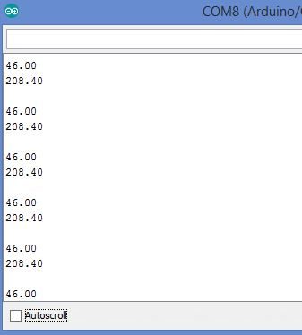
I have inserted basic uart println statements to simplify the debugging process. You have the ability to view these live by utilizing the serial monitor. The first line represents the ADC input while the second line indicates the PWM output. The maximum output is limited to 220.
Hardware
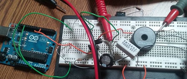
As always, here is a picture of my sloppy setup.
And the schematic
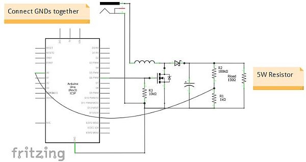
I would like to point out that Fritzing as a schematic tool is just awful. I think I’m going to go back to my regular schematic capture tools such as diptrace or OrCAD.
Make sure to connect the Arduino’s GND and your power supply’s GND together. The gate resistor to GND is to ensure it is properly turned OFF when not in use from the Arduino.
Source: Arduino DC-DC Boost Converter Design Circuit with Control Loop
