
Summary of ADI shrinks package size of 16-bit DACs
The AD5689R is a dual 16-bit voltage output DAC featuring a 2.5 V internal reference and rail-to-rail operation. It supports SPI interfaces up to 50 MHz, offers user-selectable gain (1x or 2x), and includes power-on reset logic. Available in compact 3 mm × 3 mm LFCSP or TSSOP packages, it targets applications like optical transceivers, industrial automation, and data acquisition systems with high accuracy and low drift.
Parts used in the AD5689R Project:
- Dual 16-bit rail-to-rail voltage output DAC
- 2.5 V internal reference (2 ppm/°C)
- Gain select pin (GAIN pin)
- VLOGIC pin for logic supply selection
- RSTSEL pin for reset configuration
- SPI interface (up to 50 MHz)
- Power-on reset circuit
- Per-channel power-down feature
- 3 mm × 3 mm 16-lead LFCSP package
- 16-lead TSSOP package
The AD5689R nanoDAC+™ is a dual, 16-bit, rail-to-rail, voltage output DACs. The device includes a 2.5 V, 2 ppm/°C internal reference (enabled by default) and a gain select pin giving a full-scale output of 2.5 V (gain = 1) or 5 V (gain = 2). The device operates from a single 2.7 V to 5.5 V supply, is guaranteed monotonic by design, and exhibits less than 0.1% FSR gain error and 1.5 mV offset error performance. The device is available in a 3 mm × 3 mm LFCSP and a TSSOP package.
The AD5689R also incorporates a power-on reset circuit and a RSTSEL pin that ensures that the DAC outputs power up to zero scale or midscale and remains there until a valid write takes place. Each part contains a per-channel power-down feature that reduces the current consumption of the device to 4 μA at 3 V while in power-down mode.
The AD5689R employs a versatile SPI interface that operates at clock rates up to 50 MHz, and all devices contain a VLOGIC pin intended for 1.8 V/3 V/5 V logic supplies. PRODUCT HIGHLIGHTS
- High Relative Accuracy:
AD5689R (16-bit): ±2 LSB INL max - Low Drift On-Chip Reference:
2.5 V, 2 ppm/°C temperature drift - Tiny Package:
3 mm × 3 mm, 16-lead LFCSP or 16-lead TSSOP
APPLICATIONS
- Optical transceivers
- Base-station power amplifiers
- Process control (PLC I/O cards)
- Industrial automation
- Data acquisition systems
FEATURES and BENEFITS
High relative accuracy (INL):
±2 LSB maximum @ 16 bits
Low drift 2.5 V reference:
2 ppm/°C typical
Tiny package: 3 mm × 3 mm,
16-lead LFCSP
Total unadjusted error (TUE): ±0.1% of FSR maximum
Offset error: ±1.5 mV maximum
Gain error: ±0.1% of FSR maximum
High drive capability: 20 mA,
0.5 V from supply rails
User selectable gain of 1 or 2 (GAIN pin)
Reset to zero scale or midscale (RSTSEL pin)
1.8 V logic compatibility
50 MHz SPI with readback or daisy chain
See data sheet for additional features
FEATURES and BENEFITS
- High relative accuracy (INL):
- ±2 LSB maximum @ 16 bits
- Low drift 2.5 V reference:
- 2 ppm/°C typical
- Tiny package: 3 mm × 3 mm,
- 16-lead LFCSP
- Total unadjusted error (TUE): ±0.1% of FSR maximum
- Offset error: ±1.5 mV maximum
- Gain error: ±0.1% of FSR maximum
- High drive capability: 20 mA,
- 0.5 V from supply rails
- User selectable gain of 1 or 2 (GAIN pin)
- Reset to zero scale or midscale (RSTSEL pin)
- 1.8 V logic compatibility
- 50 MHz SPI with readback or daisy chain
- See data sheet for additional features
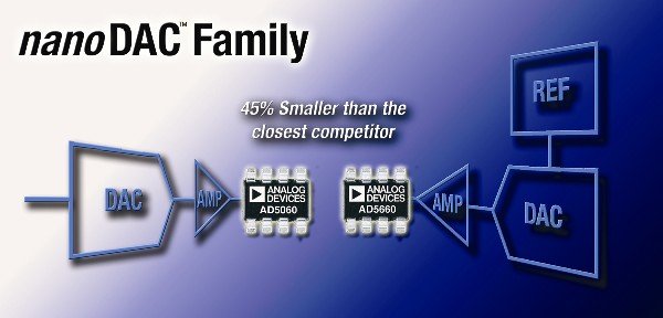
Analog Devices has introduced a 16-bit dual digital-to-analogue converter (DAC) in its nanoDAC series of small package devices.
Relative accuracy is specified at ±2-LSB INL and the device has an on-chip 2.5V reference with 2ppm/°C stability.
The AD5689R has pin-selectable functions such as VLOGIC facilitating 1.8-V, 3-V and 5-V logic levels and a GAIN pin enabling the output range to be doubled.
There are both SPI and I2C interface options.
The DAC is offerd in a 3x3mm 16-lead LFCSP and 16-bit TSSOP.
Download data sheet, order samples and evaluation boards: http://www.analog.com/AD5689R
Connect with engineers and ADI product experts on EngineerZone, an online technical support community:
For more read: ADI shrinks package size of 16-bit DACs
-
What is the resolution of the AD5689R?
The device is a dual 16-bit digital-to-analogue converter. -
Can the output range be adjusted?
Yes, a gain select pin allows a full-scale output of 2.5 V or 5 V. -
Does the device include an internal reference?
It includes a 2.5 V internal reference with 2 ppm/°C temperature drift enabled by default. -
How fast can the SPI interface operate?
The versatile SPI interface operates at clock rates up to 50 MHz. -
What logic levels are supported by the VLOGIC pin?
The VLOGIC pin facilitates 1.8 V, 3 V, and 5 V logic supplies. -
How does the device handle power-up states?
A power-on reset circuit ensures outputs power up to zero scale or midscale until a valid write occurs. -
What is the current consumption in power-down mode?
Current consumption reduces to 4 μA at 3 V while in power-down mode. -
What are the available package options?
The device is available in a 3 mm × 3 mm LFCSP and a TSSOP package.
