Summary of BROADCOM AFBR-S4N33C013 IS A SILICON PHOTO MULTIPLIER
The Broadcom AFBR-S4N33C013 is a 3.0 × 3.0 mm2 silicon photomultiplier (SiPM) in a chip-sized package using through-silicon-via (TSV) technology. It offers >54% PDE at 420 nm, high fill factor, excellent single-photon timing resolution (SPTR) and coincidence resolving time (CRT), and uniform breakdown voltage and gain. A highly transparent glass protective layer provides broad visible-to-UV sensitivity. The CSP is four-side tileable for larger-area arrays and is RoHS compliant and lead-free, optimized for detecting low-level pulsed light like Cherenkov and scintillation from common scintillators.
Parts used in the AFBR-S4N33C013:
- AFBR-S4N33C013 silicon photomultiplier (SiPM) chip-sized package (CSP)
- Through-silicon-via (TSV) technology for four-side tiling
- Highly transparent glass protective layer
- 3.0 × 3.0 mm2 active SiPM die
- 30 × 30 μm2 microcell pitch structure
- Packaging materials compliant with RoHS (lead-free)
The Broadcom® AFBR-S4N33C013 is a single silicon photomultiplier (SiPM) used for ultra-sensitive precision measurement of single photons. The active area is 3.0 × 3.0 mm2.
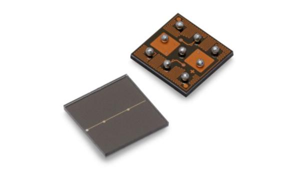
The high packing density of the single chips is achieved using through-silicon-via (TSV) technology and a chip-sized package (CSP). Larger areas can be covered by tiling multiple AFBR-S4N33C013 CSPs almost without any edge losses. The protective layer is made by a glass highly transparent down to UV wavelengths, resulting in a broad response in the visible light spectrum with high sensitivity towards blue- and near-UV region of the light spectrum.
The AFBR-S4N33C013 SiPM is best suited for the detection of low-level pulsed light sources, especially for the detection of Cherenkov- or scintillation light from the most common organic (plastic) and inorganic scintillator materials (for example, LSO, LYSO, BGO, NaI, CsI, BaF, LaBr). This product is lead-free and compliant with RoHS.
Key Features
- High PDE of more than 54% at 420 nm
- Chip-sized package (CSP)
- Excellent SPTR and CRT
- Excellent uniformity of breakdown voltage, 180 mV (3 sigma)
Additional Features
- Excellent uniformity of gain
- With TSV technology (4-side tileable), with high fill factors
- Size 3.14 × 3.14 mm2
- Cell pitch 30 × 30 μm2
- A highly transparent glass protection layer
Read more: BROADCOM AFBR-S4N33C013 IS A SILICON PHOTO MULTIPLIER
- What is the active area size of the AFBR-S4N33C013?
The active area is 3.0 × 3.0 mm2. - What package technology enables tiling of multiple chips?
Through-silicon-via (TSV) technology enables four-side tileable chip-sized packages. - What is the photon detection efficiency at 420 nm?
The device has a high PDE of more than 54% at 420 nm. - Is the AFBR-S4N33C013 suitable for detecting scintillation and Cherenkov light?
Yes, it is best suited for detection of low-level pulsed light such as Cherenkov and scintillation light from common scintillators. - What protects the SiPM surface and what is its optical property?
A highly transparent glass protective layer protects the surface and is highly transparent down to UV wavelengths. - What are the cell pitch and package size?
The cell pitch is 30 × 30 μm2 and the package size is 3.14 × 3.14 mm2. - How uniform is the breakdown voltage?
The breakdown voltage uniformity is 180 mV (3 sigma). - Is the product RoHS compliant and lead-free?
Yes, the product is lead-free and compliant with RoHS.