Summary of Creating footprints in KiCad using a scanner
This article explains how to create custom PCB footprints for proprietary components lacking CAD drawings by scanning the physical part and importing it into CAD software. The author details aligning the component on a flatbed scanner and scaling the resulting bitmap within a CAD package like QCAD to ensure precise measurements for board design.
Parts used in the Custom PCB Footprint Project:
- SD card sockets
- Flatbed scanner
- Public transport card (for alignment)
- CAD package (QCAD)
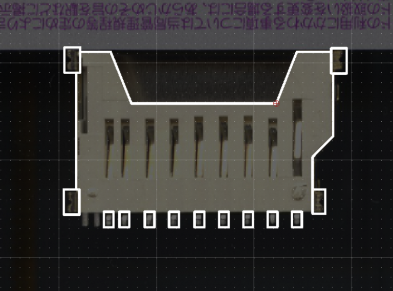
Some time ago I sourced a number of very cheap SD card sockets from China for a hobby project I was working on. Sadly, when it came to PCB design, I couldn’t find the footprints for this particular socket anywhere – the part being a proprietary invention of the factory rather than a cheap knockoff of a reputable brand like Amphenol or Molex for which drawings are readily available off of snapeda.com.
Turns out, this is a problem with many, many parts – there are no CAD drawings to be found anywhere, and the only way to really fit the part onto a board is to measure the part and draw everything yourself – a tedious manual process, but with a few tools, any part can be precisely drawn and transferred onto the board.
Step one – Scan the part using a flatbed scanner
In the absence of other tools, one can use any flatbed scanner to reproduce the measurements required to draw a part. At 300dpi, a scan will yield a sufficient measurement on most, if not all parts. One key thing to remember is to ensure that each part is aligned with the edge of the scanner – I’ve managed to accomplish this, using a public transport card I’ve found in my drawer. Simply place the card (or any other rectangular item) next to the edge, and make sure it touches it and is aligned with it, then – align your parts with the edges of the card. The alternative is to use the edges of the scanner to align the parts, but I’ve found that to be unreliable.
Step two – Open your CAD package and import the bitmap
Fire up your favorite CAD package (QCAD is my choice), and import the bitmap. Ensure that it is scaled properly – in my case (a 300 dpi) scan, the width/height factor turned out to be 0.0847 (300 dpi is 11.811 dots/mm, and 1/11.811 = 0.08466683600033867).
Read more: Creating footprints in KiCad using a scanner
- How can I fit a proprietary part onto a PCB without available drawings?
You must measure the part manually using tools like a flatbed scanner to draw the footprint yourself. - Can I use any flatbed scanner to reproduce part measurements?
Yes, a scan at 300dpi yields sufficient measurements for most parts. - What is the best way to align the part on the scanner?
Place a rectangular item like a public transport card next to the scanner edge to align the part with the card's edges. - Does the article recommend using the scanner edges directly for alignment?
No, the author found using the scanner edges to be unreliable compared to using an aligned rectangular object. - Which CAD package does the author choose for this process?
The author uses QCAD as their preferred choice. - How do you ensure the imported bitmap is scaled properly?
You must calculate the width/height factor based on the DPI; for 300 dpi, the factor is approximately 0.0847. - What calculation determines the scale factor for a 300 dpi scan?
Divide one by 11.811 (dots per mm), which results in roughly 0.08466683600033867. - Why were standard footprints unavailable for the SD card sockets?
The sockets are a proprietary invention of the factory rather than a knockoff of a reputable brand with available drawings.