Sony’s advance in image sensors appears quite natural: the company has developed a set of curved CMOS image sensors based on the curvature of the eye. A report on the sensors in IEEE Spectrum said that, “in a bit of biomimicry,” Sony engineers were able to achieve a set of curved CMOS image sensors using a “bending machine” of their own construction.
Sony’s Kazuichiro Itonaga, a device manager, reported on the new development in Hawaii, at the 2014 Symposia on VLSI Technology and Circuits. This is a conference on semiconductor technology and circuits, which took place from June 9 to June 13.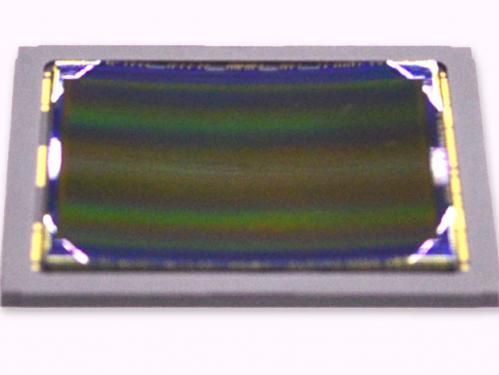
It was unclear how much the chips were curved, said IEEE Spectrum, although Itonaga said they did achieve the same level of curvature found in the human eye. The curved systems were 1.4 times more sensitive at the center of the sensor and twice as sensitive at the edge, according to the Sony engineers.
According to IEEE Spectrum, “Photodiodes at the periphery of a sensor array will be bent toward the center, which means light rays will hit them straight on instead of obliquely. What’s more, the strain induced on a CMOS sensor by bending it alters the band gap of the silicon devices in the sensor region, lowering the noise created by ‘dark current’—the current that flows through a pixel even when it is receiving no external light.” A curved CMOS sensor has an edge over a planar sensor, Itonaga noted. Considering its geometry, it can be paired with a flatter lens and larger aperture, which lets in more light.
For more detail: Sony inspired by biomimicry develops curved CMOS sensors