
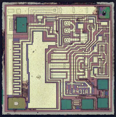
A die photo of the interesting but little-known TL431 power supply IC provides an opportunity to explore how analog circuits are implemented in silicon. While the circuit below may look like a maze, the chip is actually relatively simple and can be reverse-engineered with a bit of examination. This article explains how transistors, resistors, and other components are implemented in silicon to form the chip below.
The TL431 is a “programmable precision reference”[1] and is commonly used in switching power supplies, where it provides feedback indicating if the output voltage is too high or too low. By using a special circuit called a bandgap, the TL431 provides a stable voltage reference across a wide temperature range. The block diagram of the TL431 below shows that it has a 2.5 volt reference and a comparator[1], but looking at the die shows that internally it is quite different from the block diagram.
The TL431 has a long history; it was introduced in 1978[2] and has been a key part of many devices since then. It helped regulate the Apple II power supply, and is now used in most ATX power supplies[3] as well as the the iPhone charger and other chargers. The MagSafe adapter and other laptop adapters use it, as well as minicomputers, LEDdrivers, audio power supplies, video games and televisions.[4]
The photos below show the TL431 inside six different power supplies. The TL431 comes in many different shapes and sizes; the two most common are shown below.[5] Perhaps a reason the TL431 doesn’t get much attention because it looks like a simple transistor, not an IC.
How components are implemented in the TL431’s silicon
Since the TL431 is a fairly simple IC, it’s possible to understand what’s going on with the silicon layout by examining it closely. I’ll show how the transistors, resistors, fuses, and capacitors are implemented, followed by a reverse-engineering of the full chip.
Implementing different transistor types in the IC
The chip uses NPN and PNP bijunction transistors (in contrast to chips like the 6502 that use MOSFET transistors). If you’ve studied electronics, you’ve probably seen a diagram of a NPN transistor like the one below, showing the collector (C), base (B), and emitter (E) of the transistor, The transistor is illustrated as a sandwich of P silicon in between two symmetric layers of N silicon; the N-P-N layers make a NPN transistor. It turns out that on the chip, the transistors look nothing like this. The base isn’t even in the middle!
The photo below shows one of the transistors in the TL431 as it appears on the chip. The different pink and purple colors are regions of silicon that has been doped differently, forming N and P regions. The whitish-yellow areas are the metal layer of the chip on top of the silicon – these form the wires connecting to the collector, emitter, and base.
Underneath the photo is a cross-section drawing showing approximately how the transistor is constructed.[6] There’s a lot more than just the N-P-N sandwich you see in books, but if you look carefully at the vertical cross section below the ‘E’, you can find the N-P-N that forms the transistor. The emitter (E) wire is connected to N+ silicon. Below that is a P layer connected to the base contact (B). And below that is a N+ layer connected (indirectly) to the collector (C).[7] The transistor is surrounded by a P+ ring that isolates it from neighboring components. Since most of the transistor in the TL431 are NPN transistors with this structure, it’s straightforward to pick out the transistors and find the collector, base, and emitter, once you know what to look for.
For more detail: Reverse-engineering the TL431