Summary of Raman-on-a-chip boosts High-Resolution Handheld Spectroscopy
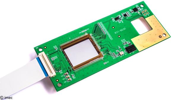
imec presents a miniaturized on-chip Raman spectroscopy solution using parallel waveguide interferometers integrated on a CMOS image sensor. This patented technology overcomes the size-performance trade-off of conventional devices, enabling high optical throughput and spectral resolution (<1nm) in handheld form factors via SiN biophotonics platforms.
Parts used in the On-Chip Raman Spectroscopy Project:
- Waveguide interferometers
- CMOS image sensor
- Silicon Nitride (SiN) biophotonics platform
- Monolithic integration system
Next week, at SPIE BIOS and SPIE Photonics West 2019 in San Francisco, imec, a world-leading research and innovation hub in nanoelectronics and digital technologies, presents an on-chip solution for Raman spectroscopy – based on a newly patented concept – providing high optical throughput and high spectral resolution. The solution could pave the way for affordable high-end handheld Raman spectroscopy device opening up many new applications. Imec invites technology partners and IDMs to further develop the technology into a commercial application.
Raman spectroscopy is a powerful technique, most often used to determine chemical and material composition. Application areas include the medical, food, even space industries. Because of the inherent nature of the technique, existing devices are rather bulky (tabletop) and have a price range of a few hundred thousand dollars/euros. Handheld solutions exist, but for the moment fail to reach the desired performance for high-end applications, largely because of the limited scaling capacity of conventional dispersive Raman spectrometry whereby scattered light is focused on a slit. Scaling while maintaining high spectral resolution (< 1nm) means reducing the size of the slit which immediately limits the optical throughput.
Thanks to a new concept, for which a patent is pending, imec has now been able to overcome this performance barrier. By massive parallelization of waveguide interferometers integrated monolithically on top of a CMOS image sensor, both high optical throughput and high spectral resolution can be reached in a miniaturized device. This novel system is built in imec’s SiN biophotonics platform which guarantees robustness and compatibility with high-volume manufacturing. Part of the work was performed under the EU-funded IoSense program.
Read more: Raman-on-a-chip boosts High-Resolution Handheld Spectroscopy
- What technique does imec present for Raman spectroscopy?
Imec presents an on-chip solution based on a newly patented concept providing high optical throughput and high spectral resolution. - How does the new concept overcome performance barriers?
It uses massive parallelization of waveguide interferometers integrated monolithically on top of a CMOS image sensor. - Can this solution enable affordable handheld devices?
Yes, the solution could pave the way for affordable high-end handheld Raman spectroscopy devices. - Does the device maintain high spectral resolution while scaling down?
Yes, the system reaches high spectral resolution of less than 1nm while reducing size. - What platform guarantees robustness and manufacturing compatibility?
The novel system is built in imec's SiN biophotonics platform which guarantees robustness and compatibility with high-volume manufacturing. - Why do existing handheld solutions fail for high-end applications?
They fail largely because of the limited scaling capacity of conventional dispersive Raman spectrometry where reducing slit size limits optical throughput.