
Summary of EEVblog #678 – What is a PCB Spark Gap?
This tutorial explains PCB spark gaps as a cost-effective method to prevent ESD damage. The author demonstrates how to design these components into a board, calculate their voltage ratings, and validates their functionality by applying 5kV to the gaps.
Parts used in the PCB Spark Gap Project:
- PCB
- Spark gap
- Power source capable of 5kV
In this tutorial Dave explains what a PCB spark gap is and how it can be a useful zero cost addition to your PCB layout to help prevent ESD damage.
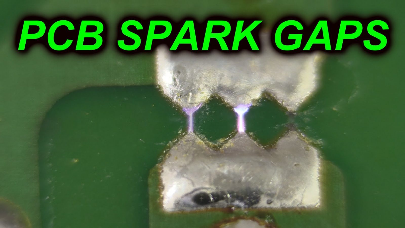
He shows how to easily design them into your board and calculate the approximate voltage rating.
And of course has some fun applying 5kV to some gaps to show how them at work.
For more detail: EEVblog #678 – What is a PCB Spark Gap?
- What is a PCB spark gap?
A useful zero-cost addition to a PCB layout designed to help prevent ESD damage. - How can you design them into your board?
The tutorial shows how to easily design them into your board and calculate the approximate voltage rating. - Does it cost money to add this feature?
No, it is described as a useful zero-cost addition to your PCB layout. - Can you apply high voltage to test them?
Yes, the author applies 5kV to some gaps to show them at work. - What is the best way to determine voltage rating?
You can calculate the approximate voltage rating when designing them into the board. - What problem does this component solve?
It helps prevent ESD damage on the circuit board.