Abstract—This paper discusses the essential steps taken to achieve a low-EMI prototype before conducting compliance tests in an anechoic chamber. These steps include electronic circuit design for minimal radiation, and pre-compliance inspections. The pre-compliance inspections include simulated EMI analysis of a printed circuit board (PCB) layout model using 3DEM software, and a near-field EM scan of the prototype PCB using a spectrum analyzer (SA). Success is confirmed by anechoic testing.
I. Circuit Design for Minimum EMI
In order to achieve a low radiated emission (RE), some best practices to design electronic circuit and PCB layout have to be applied. These practices include EMI filtering by adding ferrite beads to the signals like power rails, data lines of USB, Ethernet, and so on. Furthermore, sufficient quantity of decoupling capacitors have to be properly placed along the power rails to minimize the power network impedance, which in turn reduces the amplitude of noise ripple contributed by the digital load, and poses a lower risk of radiation. On the other hand, the closed-loop compensation network of the switch mode power supply has to be properly designed to achieve a stable closed-loop, so that the oscillation at the voltage output is controllable, and in turn minimizes the magnitude of the switching noise ripple. A smaller noise ripple reduces the risk of EMI of the prototype.
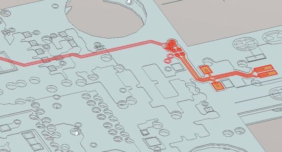
Besides that, PCB traces of signals with high frequency or edge rate shall be referenced to a continuous return path (i.e., reference ground plane) to reduce the risk of EMI too. The trace shall not cross any split planes and voids. Whenever there is signal transition from one layer to another through a via, there shall be at least one stitching via placed by the side of the signal via. The stitching via serves as a proper guided path for the return signal current to propagate back from the receiving end to the transmitting end. Without a proper reference path, the return current could travel to any point within the PCB and become a potential source of EMI.
For more detail: Build low-EMI prototypes: The essentials