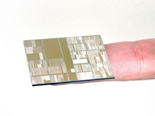
IBM shows working devices fabricated at 7nm node
Continuing semiconductor scaling down to feature sizes of 7 nm is expected to yield further gains in performance, and lower power levels, but in IBM’s words, “[its] researchers had to bypass conventional semiconductor manufacturing approaches”. The finFET-style transistors in the demonstrator were constructed with silicon-germanium (SiGe) channels, and the lithography that defined them employed Extreme […]
IBM shows working devices fabricated at 7nm node Continue Reading