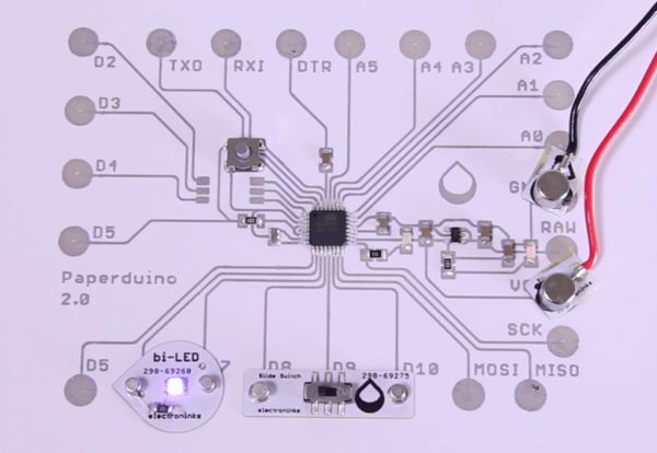
What if making an Arduino, or wiring up an Arduino was as easy as printing one out? In this tutorial we printed our own Arduino Pro Mini board using a pen plotter and the Electroninks Circuit Scribe (a rollerball pen with highly conductive ink). Within 15 minutes we printed the board, placed components down with glue or tape, and uploaded a sketch.
Paperduino 2.0 with Circuit Scribe
Materials needed:
Circuit Scribe conductive ink pen
Silhouette SD plotter
8.5×11″ glossy photo paper
Electroninks Arduino connection kit
FTDI cable
USBtinyISP bootloader or a pre-bootloaded Arduino chip
Superglue (Loctite gel) or Z-tape[/su_box]
Software:
EAGLE PCB (if you want to modify the board)
Arduino IDE
Silhouette Studio
Downloads:
Paperduino 2.0 Schematics and Layout (EAGLE)
Components list:
View BOM (ordering list) on Google Spreadsheet
2x 10 uF capacitors (1206 package)
3x 0.1 uF capacitor (1206)
2x 10 KOhm resistors (1206)
330 Ohm resistor (1206)
ATmega328P-AU
Red LED (1206)
Green LED (1206)
5V voltage regulator (5 pin)
8 MHz resonator
Tactile switch
Step 1: Editing the layout in EAGLE
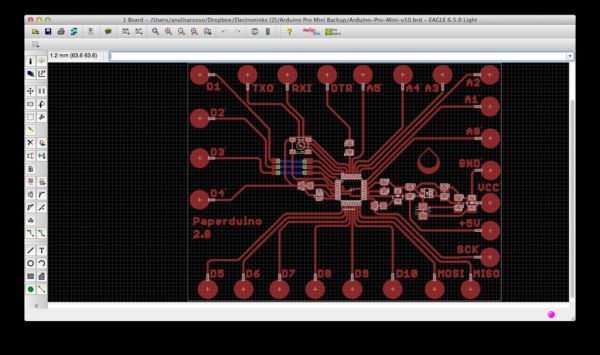
Our Paperduino design is based on the open source design for the Arduino Pro Mini. We used EAGLE PCB to design the board.
Download a schematic
The Arduino Pro Mini board schematic can be found on the Arduino website.
Our final Paperduino 2.0 EAGLE files can be found here.
Adapting the board for paper
In order to make the schematic paper-friendly, we replaced the blocks of pin headers with our own custom round pad. Through-hole components such as the pin headers are difficult to use on flexible surfaces like paper. We added the new pad design to our Electroninks component library. Since the pen plotter only prints lines, but not fill patterns, the pads were composed of overlapping concentric circles. The tool path for plotting will be shown in Step 3.
We also replaced the package for many of the small components with the 1206 package (meaning 1.2mm long x 0.6mm wide) so they would be easier to mount later on.
Designing the board layout
In the board layout, we set the top layer line width to 0.6 mm to match the width of the pen trace.
We designed the board layout so the Paperduino could be printed on one layer. In many cases, the surface mount components act as jumpers. It is important to keep components close together to minimize line resistance between them.
In EAGLE PCB, the component pads will not be filled in by the pen plotter when exported as a DXF — only the outlines will be drawn. To solve this issue, overlay the pads with meandering line features so they will be filled by a raster pattern.
Finally, if any lines require a paper jumper (like our digital pins 1, 2, and 3), they can be created in the bottom layer (blue). After the first layer is printed, paper stickers can be place over the lines and the bottom DXF layer can be used to print over the stickers. We will publish a jumper sticker tutorial in a future Instructable.
For more detail: Paperduino 2.0 with Circuit Scribe


