
Summary of LTC6752 – 280MHz, 2.9ns Comparator Family with Rail-to-Rail Inputs and CMOS Outputs
The LTC6752 family comprises very high-speed comparators with up to 280 MHz toggle rate, 2.9 ns propagation delay, 1.2 ns rise/fall times, rail-to-rail inputs, and ±22 mA output drive. Options include separate input/output supplies, single-supply variants, shutdown, output latch, adjustable hysteresis, and complementary outputs. Low jitter and dispersion suit clock recovery, line receivers, and high-speed data systems. Available in multiple packages and direct replacement for ADCMP60X, they operate from –40°C to 125°C.
Parts used in the LTC6752 Comparator Family Project:
- LTC6752 comparator family devices (5 members with varying features)
- TSOT-23 package
- SC70 package
- MSOP package
- 3mm × 3mm QFN package
- Separate input and output supply option (2.45V to 5.25V input, 1.71V to 3.5V output)
- Single supply option (2.45V to 3.5V)
- Shutdown pin feature
- Output latch feature
- Adjustable hysteresis
- Complementary outputs
Features
- Very High Toggle Rate: 280MHz
- Low Propagation Delay: 2.9ns
- Rail-to-Rail Inputs Extend Beyond Both Rails
- Output Current Capability: ±22mA
- Low Quiescent Current: 4.5mA
- Features within the LTC6752 Family:
- 2.45V to 5.25V Input Supply and 1.71V to 3.5V Output Supply (Separate Supply Option)
- 2.45V to 3.5V Supply (Single Supply Option)
- Shutdown Pin for Reduced Power
- Output Latch and Adjustable Hysteresis
- Complementary Outputs
- Packages: TSOT-23, SC70, MSOP, 3mm × 3mm QFN
- Direct Replacement for ADCMP60X Family
- Operating Temperature Range: –40°C to 125°C
Description
The LTC®6752 is a family of very high speed comparators capable of supporting toggle rates up to 280MHz. These comparators exhibit low propagation delays of 2.9ns, and fast rise/fall times of 1.2ns. There are a total of 5 members in the LTC6752 family, with different options for separate input and output supplies, shutdown, output latch, adjustable hysteresis, complementary outputs, and package.
The LTC6752 comparators have rail-to-rail inputs that operate from 2.45V, up to 3.5V or 5.25V, depending on the option. The outputs are CMOS and the separate supply options can operate down to 1.71V, allowing for directly interfacing to 1.8V logic devices.
The low propagation delay of only 2.9ns combined with low dispersion of only 1.8ns (10mV to 125mV overdrive variation) makes these comparators an excellent choice for critical timing applications. Similarly, the fast toggle rate and the low jitter of 4.5ps RMS (100mVP-P, 100MHz input) make the LTC6752 family ideally suited for high frequency line driver and clock recovery circuits.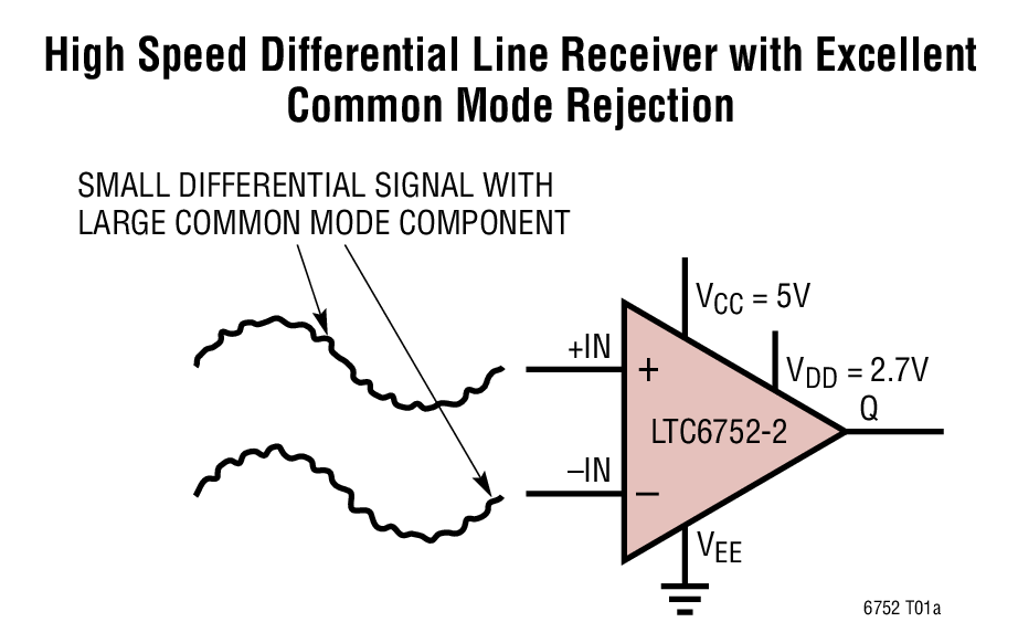
Applications
- Clock and Data Recovery
- Level Shifting
- High Speed Data Acquisition Systems
- Window Comparators
- High Speed Line Receivers
- Fast Crystal Oscillators
- Time of Flight Measurements
- Time Domain Reflectometry
People Who Viewed This Product Also Viewed
- LTC6957 – Low Phase Noise, Dual Output Buffer/Driver/Logic Converter
- LT1028 – Ultra Low Noise Precision High Speed Op Amps
- LT4320/LT4320-1 – Ideal Diode Bridge Controller
- LT1719 – 4.5ns Single/Dual Supply 3V/5V Comparator with Rail-to-Rail Output
- LTC6409 – 10GHz GBW, 1.1nV/√Hz Differential Amplifier/ADC Driver
- LTC6268 – 500MHz Ultra-Low Bias Current FET Input Op Amp
- LTC6268-10 – 4GHz Ultra-Low Bias Current FET Input Op Amp
- LT3080 – Adjustable 1.1A Single Resistor Low Dropout Regulator
- LTC6655 – 0.25ppm Noise, Low Drift Precision References
- LT5400 – Quad Matched Resistor Network
For more detail: LTC6752 – 280MHz, 2.9ns Comparator Family with Rail-to-Rail Inputs and CMOS Outputs
- What is the maximum toggle rate of the LTC6752?
The LTC6752 supports toggle rates up to 280MHz. - What is the propagation delay of the LTC6752?
The LTC6752 has a low propagation delay of 2.9ns. - Do the LTC6752 inputs support rail-to-rail operation?
Yes, the LTC6752 comparators have rail-to-rail inputs. - What output current capability does the LTC6752 provide?
The LTC6752 output current capability is ±22mA. - Can the LTC6752 interface directly to 1.8V logic?
Yes, separate supply options allow outputs down to 1.71V for direct interfacing to 1.8V logic devices. - What features are available in the LTC6752 family?
Features include separate or single supply options, shutdown pin, output latch, adjustable hysteresis, and complementary outputs. - What packages are available for the LTC6752?
Packages include TSOT-23, SC70, MSOP, and 3mm × 3mm QFN. - What applications are suitable for the LTC6752?
Applications include clock and data recovery, level shifting, high speed data acquisition, window comparators, high speed line receivers, fast crystal oscillators, time of flight, and time domain reflectometry. - What is the operating temperature range of the LTC6752?
The LTC6752 operates from –40°C to 125°C.
