Topics:
1. First Build
It would be a really good idea to build this circuit before going to the lab because it is time consuming to connect all of the wires.
1.1 The Circuit
The circuit here is CIRC-05, from your book. For formality, the schematic diagram is the following:
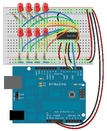
Your breadboard might look something like this:
Note:
- The shift register has a little notch missing at the “top”. That notch on the right in this diagram.

1.2 The Code
The code for this circuit is available at the following address: http://ardx.org/src/circ/CIRC05-code.txt
You can use Command-a to select everything, Command-c to copy from your Safari window, and Command-v to paste it into your Arduino window.
The code that immediately runs looks like this (notice that some functions are missing):
/*     ---------------------------------------------------------
 *     |  Arduino Experimentation Kit Example Code             |
 *     |  CIRC-05 .: 8 More LEDs :. (74HC595 Shift Register)   |
 *     ---------------------------------------------------------
 *
 * We have already controlled 8 LEDs however this does it in a slightly
 * different manner. Rather than using 8 pins we will use just three
 * and an additional chip.
 *
 *
 */

//Pin Definitions
//Pin Definitions
//The 74HC595 uses a serial communication
//link which has three pins
int data = 2;
int clock = 3;
int latch = 4;

/*
 * setup() - this function runs once when you turn your Arduino on
 * We set the three control pins to outputs
 */
void setup()
{
  pinMode(data, OUTPUT);
  pinMode(clock, OUTPUT);
  pinMode(latch, OUTPUT);
}

/*
 * loop() - this function will start after setup finishes and then repeat
 * we set which LEDs we want on then call a routine which sends the states to the
 * 74HC595
 */
void loop()                     // run over and over again
{
  int delayTime = 100; //the number of milliseconds to delay between LED updates
  for(int i = 0; i < 256; i++){
   updateLEDs(i);
   delay(delayTime);
  }
}

/*
 * updateLEDs() - sends the LED states set in ledStates to the 74HC595
 * sequence
 */
void updateLEDs(int value){
  digitalWrite(latch, LOW);     //Pulls the chips latch low
  shiftOut(data, clock, MSBFIRST, value); //Shifts out the 8 bits to the shift register
  digitalWrite(latch, HIGH);   //Pulls the latch high displaying the data
}
2. Hardware Theory
If you recall, last lab involved eight LED’s and used eight output pins (one for each LED). To expand this circuit to 16 LEDs, you would use 16 output pins. Do you detect a problem with this? (remember we only have 14 output pins).
This week, we have the same number of LED’s (eight), but we only use three of the output pins. The magic that makes this happen is the Shift Register. In fact, you can chain shift registers together to control multiples of eight LEDs (for instance 16, 24, 32, etc) and still only use three output pins.
WOW…Let’s find out how this magic Shift Register works.
2.1 Overview–“Rollover Rollover”
The concept of a shift register, brings to mind the nursery song: http://www.youtube.com/watch?v=WqF0ev8UOB4. Well, it’s not quite this idea. But now that you have this ridiculous image in your head, you might remember the concept behind shift registers.
The idea is that a “rollover” occurs and one on the edge falls out. The part that is missing in this idea is that there are others that are added to the other side. Bits (sequences of 1’s and 0’s) are the things that perform the rolling over. For instance, if we start with a pattern like this:
| 0 | 0 | 0 | 0 | 0 | 1 | 0 | 1 |
|---|
and want to end up with this pattern:
| 0 | 0 | 1 | 1 | 0 | 0 | 1 | 1 |
|---|
The sequence of “shifts” (the more technical term for “rollovers”) could be represented as follows. Notice that the movement of the bits is toward the left.
| bit shifted out | pattern of bits | bit shifted in | ||||||||
|---|---|---|---|---|---|---|---|---|---|---|
|
||||||||||
| 0 |
|
0 | ||||||||
| 0 |
|
0 | ||||||||
| 0 |
|
1 | ||||||||
| 0 |
|
1 | ||||||||
| 0 |
|
0 | ||||||||
| 1 |
|
0 | ||||||||
| 0 |
|
1 | ||||||||
| 1 |
|
1 |
We can also imagine that there is some “bell” or alarm that triggers this shift to occur. This “bell” is actually referred to as a clock. The change in the clock from LOW to HIGH is the trigger that causes the shift to occur.
2.2 What is a Shift Register
A shift register may look complicated, but just remember that ten of the pins are for the pattern (i.e. eight pins for the pattern, one for the shift in, and one for the shift out), two of the pins are for power and ground, and the remaining pins are to control the pattern.
Let’s look at a diagram and examine the pieces of a shift register:
The pieces of this diagram that are data related are:
- Q0 to Q7 (pin 1 to 7 and 15) are the eight pins containing the pattern. These pins are also know as the “output pins”
- Q7′ (pin 9) is the bit that gets rolled (or shifted) out.
- DS (pin 14) is the bit that is getting rolled (shifted) in.
The pieces that are power and ground related are:
- GND (pin 8) is (you guessed it) connected to ground
- VCC (pin 16) is connected to 5V
The remaining four pins are used to control the pattern in the shift register:
- MR (pin 10) is the “Master Reclear”.
- It will “empty” the whole shift register if pulled LOW. Notice that in our starting circuit, this pin is connected to 5V. This is because it must be pulled to HIGH to enable the shift register.
- SH_CP (pin 11) is the “SHift register Clock Pin”.
- When this pin is pulled HIGH, it will shift the register. This pin will alternate between HIGH and LOW. In our analogy, this is like the “bell” that indicates that a change will occur.
- ST_CP (pin 12) is the “STorage register Clock Pin”.
- Needs to be pulled to HIGH to have the “pattern” of bits be output by the shift register. This will be pulled HIGH after SH_CP has gone LOW. This pin will alternate between HIGH and LOW as well. This pin could be analogous to a “display” trigger. You could have multiple shifts, but only display the ending pattern.
- OE (pin 13) is the “Output Enable” pin.
- This pin enables the output when tied to GND and disables output when HIGH. Notice how our circuit has pin 13 tied to ground.
2.3 How the Arduino Controls the Shift Register
In our implementation, we have three pins connecting the Arduino to the shift register:
- DS (the bit to be shifted in)
- ST_CP (the clock that controls when the output gets displayed)
- SH_CP (the clock that controls when the shifting occurs)
These three are related as follows:
When the signal on the SH_CP-pin goes HIGH, all the values get shifted and a new value (from DS) gets shifted in. When you want the “pattern” that has been created to be output, you must also change the ST_CP pin to HIGH. This updates the output-pins with the new data.
If you are interested and would like to see the step by step interaction of these pieces (with the patterns from Section 3.1), some code is available for you in this file: shift_ Clocks.html
3. Software Theory
3.1 The shiftOut Function
Let us take a look at the partial code that runs when we copy code from http://ardx.org/CODE05
//----------------->comments cut here<-----------------

int data = 2;
int clock = 3;
int latch = 4;

//----------------->constants and setup function cut here<-----------------

void loop()                     // run over and over again
{
  int delayTime = 100; //the number of milliseconds to delay between LED updates
  for(int i = 0; i < 256; i++){
   updateLEDs(i);
   delay(delayTime);
  }
}

/*
 * updateLEDs() - sends the LED states set in ledStates to the 74HC595
 * sequence
 */
void updateLEDs(int value){
  digitalWrite(latch, LOW);     //Pulls the chips latch low
  shiftOut(data, clock, MSBFIRST, value); //Shifts out the 8 bits to the shift register
  digitalWrite(latch, HIGH);   //Pulls the latch high displaying the data
}
Notice that the updateLEDs function is called from loop. There are a couple of special functions called that relate to the shift register:
- digitalWrite(latch, LOW); Remember that we have a ST_CP pin. This is one of the clock pins, which is otherwise know as the latch. When the latch is low, we will not see the output pattern change until the latch is set to HIGH with the call to: digitalWrite(latch, HIGH);
- shiftOut(data, clock, MSBFIRST, value); This function will perform eight shifts so that a byte (value) of information can be stored in the shift register. The arguments to the function can be described as follows:
- data –This is the Arduino pin hooked up to the DS (data to be shifted in) pin of the shift register. It will be a bit at a time of the value.
- clock — This is the Arduino pin hooked up to the SH_CP (shift clock) pin of the shift register. It will toggle eight times to store the value.
- MSBFIRST — This specifies whether the value will be store in MSBFIRST (most significant bit first) or LSBFIRST (least significant bit first). You can change the code to LSBFIRST and see what happens to the pattern of lights.
- value — This is the value that you want to output. It is eight bits (one byte) of information.
Notice how value is 0 to 255, and we can see how the light pattern changes. A bubbly effect is created(no, this isn’t the technical term).
If you were overwhelmed by this talk of bits and bytes, let us take a closer look at binary numbers which are the magic behind making this code work.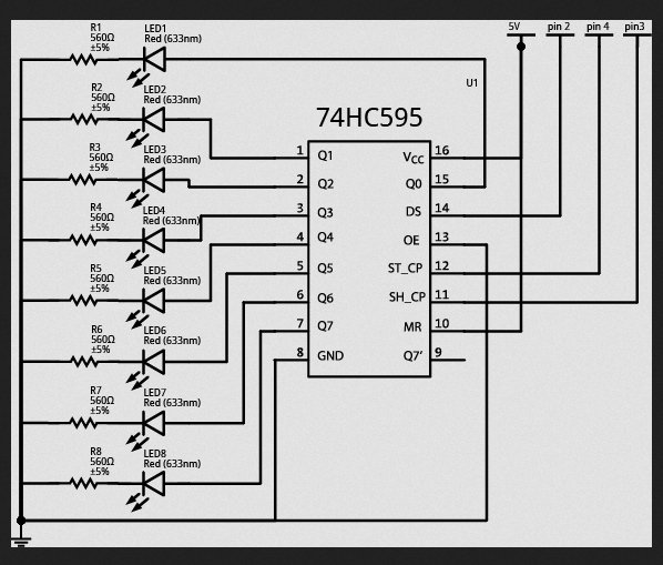
3.2 Binary Numbers
Binary numbers use only zeros and ones to represent a value. This is also known as “base 2” representation because all numbers will be represented by only 2 digits (0 and 1). By contrast, on a daily basis, we use decimal numbers, known as “base 10”. Why is it called base 10? Because we use 10 digits (0 through 9) to represent all numbers.
Usually if you take a low level programming class such as CS201, you are requested to memorize at least the first 16 values in binary. The following table summarizes this:
| binary | decimal | binary | decimal | |
|---|---|---|---|---|
| 0000 | 0 | 1000 | 8 | |
| 0001 | 1 | 1001 | 9 | |
| 0010 | 2 | 1010 | 10 | |
| 0011 | 3 | 1011 | 11 | |
| 0100 | 4 | 1100 | 12 | |
| 0101 | 5 | 1101 | 13 | |
| 0110 | 6 | 1110 | 14 | |
| 0111 | 7 | 1111 | 15 |
What is the point of this. Well, notice the bubbly pattern that happens. If you are having trouble matching the binary numbers in the table with what is happening in the Arduino, change the for loop in the loop function from 256 to 16 and increase the delay time(to say 400). You should then be able to clearly see the binary patterns in the table above. The 1’s will be represented by an on LED and the 0’s by an off LED.
So, now some terminology:
For more detail: Lab 8: Shift Register and Binary