
Summary of UnDecima Audio Output from Arduino
The UNDECIMA project is a 12-channel audio system using an Arduino Uno to create an acoustic phase array. It features one master channel and 11 linearly delayed "puppet" channels. The hardware utilizes a DAC1022 for 10-bit digital-to-analog conversion, buffered by LF351 op-amps and routed through 74HC4051 analog switches with sampling capacitors. Software manages interrupts at 40 kHz to handle data input from A5 and output via 16 digital pins, overcoming PWM speed limitations for high-quality audio.
Parts used in the UNDECIMA Project:
- Arduino Uno board
- DAC1022 10-bit multiplying digital analog converter
- LF351 operational amplifier (OPA)
- NE5532 operational amplifier
- 74HC4051 8-channel analog switches
- Sampling and hold capacitors (0.01 uF and 0.12 uF total)
- Potentiometers (for variable voltage references)
I already have one project where arduino outputs audio signal to USB speakers via software 10-bits PWM. In first, I was not satisfied with quality of sound generated via PWM. There are just not enough speed in arduino engine to run PWM well. For example for 20.000 Hz audio, PWM has to be at least 2 – 3 times higher above normal frequency range, or 40 – 60 kHz. If we multiply this value with 10-bits resolution, we would get 40 – 60 MHz, that is too much for small arduino to drive.
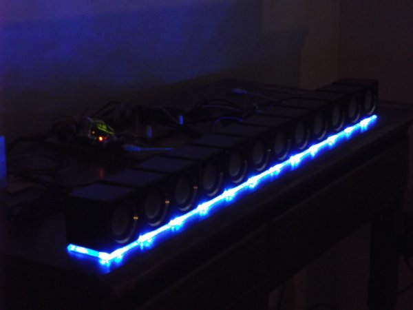
In second, the idea to create multichannel audio system was boggling my mind for about a year now. This is how UNDECIMA project was born. 1 + 11, or 12 channel !!! audio system running on arduino UNO board with full 10-bits resolution – maximum available with internal ADC. Project gets its name because there is 1 Master channel, and 11 linearly delayed copy of the same audio stream, or Puppets channels, In its essence, this is acoustic Phase Array.
As you can see on posted drawings, the “heart” of the project is 10-bit multiplying (parallel) digital analog converter DAC1022. Output of the IC than buffered with OPA and “demultiplex’d” via two 74HC4051 8-channel analog switches. Outputs of the switches loaded by sampling and hold capacitors 0.01 uF, to filter out unwanted sampling frequency noise. DAC is configured for single supply power line. Usually, they recommend to buffer output with / high input impedance / high slew rate / rail – to – rail / OPA in such configuration. Which I don’t have, and it costs about half a price of DAC itself, So, this is why I implemented two variable voltage references based on NE5532 and couple of pots. Difference in voltages between two references forms a “span”. Lower voltage creates an off-set for cheap non rail-to-rail OPA LF351, with adequate slew rate 13 V/usecond. OPA is heavily loaded by sampling and hold capacitors, which it sees as connected in parallel at its output, 0.12 uF overall! To minimize distortion level due overloading of the OPA, span couldn’t be adjust too wide, and preset in current design 1.414 V, providing exactly 1V RMS output for pure sine wave. I know, that 12 buffers / filters inserted after switches would solve a problem, but idea to solder more than 100 electronics components on a breadboard doesn’t look attractive for me.
( *I will try to find another IC / circuits capable to drive big capacitive load later on. )
SOFTWARE.
Software part of the project is straightforward ”sample-delay-output” function, completely wrapped inside interrupt subroutine. Main loop is empty. In setup 16 digital pins configured as outputs, 10 of them represent data bus, 5 are address bus and last one is check-point to measure performance with oscilloscope. Timer 2 defines a “heartbeat”, and fires interrupt every 25 usec, or at 40 kHz. ADC configured to take samples on analog input A5 (first 4 analog pins belong to data bus). Conversion prescaler: 1 MHz, allowing sampling to be completed with fast speed. I left two digital pins D0 and D1 free, as my initial attempts to use them in data bus failed.
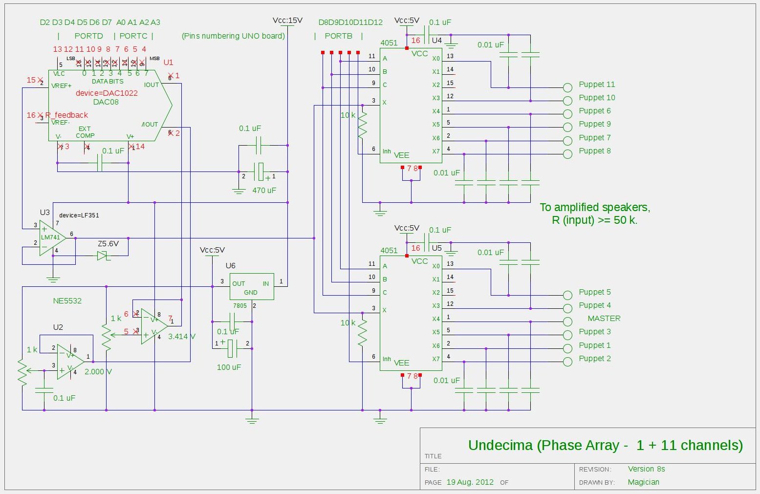
Arduino periodically refuses to reload updates, I’m not sure if it’s Linux problem or on-board USB/RS232 converter. Each sample, received from the ADC, is shifted left on two bits to skip D0 and D1, and plus one bit more (3 bits left shift overall) to fix “imperfection” of input preamplifier stage, as NE5532 (again) “non rail-to-rail” OPA. Look for drawings in “Audio Input” blog. Measurements show that each channel is receiving a data for about 1 usec “window”, which is quite fast, nevertheless not fast enough to run 16 channels or to do something else with data before sending them out. In current hardware implementation the “bottle neck” is OPA, as DAC has settling time only 500 nanoseconds.
Link to arduino UNO sketch: UnDecima.
To be continue….
For more detail: UnDecima Audio Output from Arduino
- How does the UNDECIMA project achieve 12-channel audio?
The system uses one master channel and 11 linearly delayed copies of the same audio stream. - Why was PWM not suitable for the initial audio project?
Arduino engines lack the speed to run PWM at the required 40–60 kHz frequency for 20,000 Hz audio with sufficient resolution. - What is the role of the DAC1022 in this design?
The DAC1022 serves as the heart of the project, acting as a 10-bit multiplying parallel digital analog converter. - How are the outputs demultiplexed and filtered?
Outputs are demultiplexed via two 74HC4051 switches and loaded by 0.01 uF sampling and hold capacitors to filter noise. - What voltage span is preset in the current design?
The preset span is 1.414 V, which provides exactly 1V RMS output for a pure sine wave. - At what frequency does Timer 2 fire the interrupt?
Timer 2 fires an interrupt every 25 usec, resulting in a 40 kHz heartbeat. - Which analog pin is configured for taking samples?
Analog input A5 is configured to take samples, while the first four analog pins belong to the data bus. - What is identified as the main bottleneck in the current hardware implementation?
The operational amplifier (OPA) is the bottleneck because it is heavily loaded by capacitive loads, despite the DAC having a faster settling time.
