Hey Everyone what’s up!
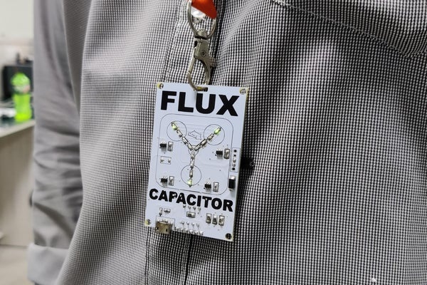
So this is my “FLUX Capacitor” PCB Badge which is a replica of the actual Flux Capacitor which was in back to the future movie.
The Flux Capacitor was the core component of Dr. Emmett Brown’s time-traveling DeLorean time machine which makes time travel possible.
Also, the Flux Capacitor in the movie required 1.21 Gigawatts of power to Run which was supplied via the plutonium nuclear reactor which was later replaced by Mr. Fusion.
Supplies
We Required the following components for this Badge Built-
- Custom PCB (which was provided by PCBWay)
- LEDs 06038205S Mosfet IC
- 10K Resistance 0805
- M7 Diode
- Attiny85
- USB Micro Port
- 1K Resistance
- Lithium CR2032 Cell SMD Holder
- Solder paste
- Arduino as ISP Programmer setup (consist of Arduino Nano or UNO)
Step 1: Energy Consumption
My Version is smaller and only requires 2.6V at 0.0069A which is around 0.017 Watts or 0.000000000017 Gigawatts which is pretty low if compared with the actual Flux Capacitor.
It runs on a 3V CR2032 Lithium Coin Cell or it can be powered by an onboard Micro USB Port. (also this is my first PCB Badge) LEDs are controlled by 8205S MOSFET IC and the gate of MOSFET IC is controlled by an Attiny85 MCU.
Step 2: Schematic
Above is the schematic of the actual Flux Capacitor which was made DOC Brown, Along with the schematic of my edition.
Step 3: Built Process and PCB Ordering
I prepared PCBs for this project in my OrCad PCB Editor and after fining this PCB I sent the Gerber data to PCBWay for samples and received them after few weeks,
I have to say PCBs that I got were great as expected! PCBWay, you guys rock.
check out PCBWay for great PCB service at less cost.
Step 4: PCB Assembly
Next is the PCB Assembly process which will include adding solder paste to each component’s pads and then pick and place each component on their assigned place process and at last the hotplate reflow process.
Step 5: Solder Paste
After Receiving the PCB, all that left to do was to apply solder paste to each component pad.
I used a normal Sn-Pb solder paste which has a melting temp from 140 to 270 °C
After Adding solder paste, we need to do the “PICK and Place Process”
Step 6: “PICK and Place Process”
I then used an ESD Tweeaser to carefully pick and place each component on their assigned place one by one which took like 3 mins top but end result was a perfect PCB with all the components place in their place in the right orientation.
(we are using LEDs here so be extra careful when placing them in their assigned place, talking about polarity here)
Step 7: Hotplate
After the “PICK and Place Process”, I carefully lifted the whole circuit board and place it on my DIY SMT Hotplate which is also homemade just like this project.
https://www.instructables.com/DIY-SMT-Hotplate-Pro…
After Few mins when the hotplate reaches the Solderpaste melting TEMP, all the components will get soldered by this Hot Reflow process and Our Flux Cap PCB will be completed.
Now let’s flash the attiny85 and finally run this sucker.
Step 8: Code
As for the Code, I’m using this modified chaser sketch.
Step 9: Arduino As ISP
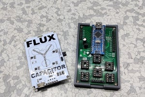
I have used this Arduino as an ISP programmer which I made last year. it’s basically an Arduino nano that has its SPI Pins breakout for connecting Attiny85 or Attiny13A with it in order to flash the Attiny MCU. If you want to know how this setup works then definitely check out this post of mine.
https://www.instructables.com/Multiple-ATtiny8513A…
- We connect the VCC of the Arduino as ISP to the VCC of Attiny,
- GND to GND
- Reset to pin D10 (of Arduino Nano)
- Mosi to pin D11 (of Arduino Nano)
- Miso to D12 (of Arduino Nano)
- and SCK to D13 (of Arduino Nano)
As soon as I powered this setup, Middle LED started blinking, Reason for that was- I have previously flashed a Blink Sketch to this MCU so we can see the Blinking of the D0 pin of Attiny85.
To Flash Code to the Attiny85, we first need to wire the Arduino as ISP setup with the Custom PCB Badge in the above configuration.
- We first select the right MCU which is attiny85 in our case and do not forget to choose the right com port.
- then we select the right programmer which is in our case “Arduino as ISP”
- then we hit on the Burn Bootloader option which will take few seconds
After Burning the bootloader, the Previously Flashed Blink SKetch in Attiny85 is now erased completely and the LEDs stopped Blinking,
- Now we go to the sketch menu and select the “Upload using Programmer” Option and BANG.
you have successfully uploaded a sketch to this Attiny85 MCU.
Step 10: Result and Conclusion, Also Additional Stuff
These are few points I concluded from this built-
- Making PCB Badge is a pretty easy thing to do
- CR2032 cells are not suited for constantly powering so many LEDs at the same time
- This setups barely resembles the original Flux Capacitor
- Attiny85 is the best low-cost MCU but an Attiny13A can be used here which will also save cost.
This badge can also be equipped with an ID card strap and we can wear it like a HiGh tech ID Card, pretty cool right?
Also, I have modeled this PCB in Fusion 360 and then prepared a base body around it and then 3D Printed it. after that, I just screw the Badge on its 3D Printed Body.
that’s all for now, leave a comment if you need any help with this project!
Source: Flux Capacitor PCB Badge