Summary of PCB Development – You May Not Know About The Future Trends!
The article explores how the Internet of Things (IoT) is revolutionizing Printed Circuit Board (PCB) development. It highlights a shift toward flexible and High-Density Interconnect (HDI) boards to create smaller, more efficient devices like smartwatches and wearables. Key trends include rigid-flex designs, advanced packaging technologies like Multi-Chip Modules, and improved wireless connectivity. The text emphasizes the need for closer collaboration between mechanical and electronic designers, enhanced power management strategies, and materials that withstand environmental factors such as moisture and heat.
Parts used in the IoT PCB Development Project:
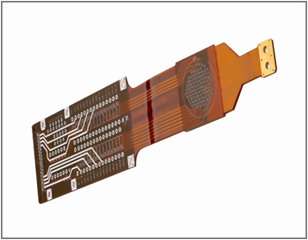
- Flex PCBs
- HDI (High-Density Interconnect) boards
- Rigid flex circuit assemblies
- Signal trace layers
- Copper weight components
- Stiffeners
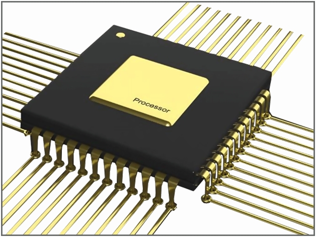
- Multi-Chip Modules
- System-in-Package models
- Wireless modules
- RF circuits
We have finally reached the era of IOT (Internet of Things) and it’s all over the place on practically every nook and cranny of the world. According to professionals, IoT can be illustrated as two things- the fourth industrial upheaval and the greatest thing that has happened since the eruption of .com.
With the latest update gathered by Gartner, in the year 2020, the earth is likely to possess not less than 20 billion devices enabled by the internet as regards PCB development.
With this new technological innovation, many great developers have started emerging with different brilliantly linked avenues which include smart cars, wearable equipment, medical detection tools, and so on.
IoT tends to offer a lot to everyone. It provides a promising and propitious opportunity, establishing a link between the physical factors as well as the virtual components. In this article, we’ll be learning about both the growth and future of IoT. Get ready to be enlightened!
QUICK SURVEY
Internet of Things Leading Towards New Advances to PCB Development
Formulation of new PCB Innovations for Internet of Things: What’s new?
The Link Between IoT and Impending PCB Development.
Conclusion
1. Internet Of Things Leading Towards New Advances To PCB Development
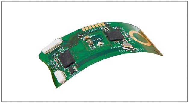
One of the most recent updates as regards PCB developments is the surprising and undeniable utilization of flex and HDI boards. I mean it is all over the place. The initial plan and design of IoT devices was to be utilized when moving from one place to another and the utilization of flex PCBs improves wiring while at the same time giving additional opposition from unfavorable situations.
Additionally, most developers have started to use HDI methods due to the decline in BDA (Board Surface Area) and increase in routing density in order to save some important space. Another advantage is that these so called HDI developments consume less power and perform much better, thereby making better IoT devices. In other words, the use of HDI methods is a better option than the latter due to its added advantages.
So making use of both flex and HDI advances to PCB developments, tech companies can now develop small mobiles devices that are less vulnerable to harsh conditions such as heat and loss of signal, without affecting its performance and workability. With this new innovation and advancement to PCB developments, this gives room for an opportunity to develop new IoT devices in smaller sizes, less weighty with quicker performance.
2. Formulation of new PCB Innovations for Internet of Things: What’s new?
We cannot say that IOT has brought about the total revolution in the development of PCB’s. What we can and are certain about is that it has brought new ideas that can be considered to the table.
Due to the various kind of design advances, the arrangements, formulation and the procedure of bringing together an IoT-based PCB, that is entirely different from that of the normal conventional board.
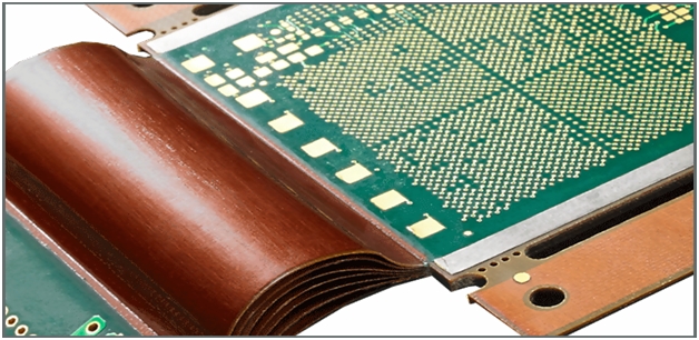
Typically, when comparing the composition of IoT PCB’s, we can say the new designs involve either of the following: Rigid flex or flex circuit assemblies. These compositions make it entire different from its normal state which was bigger and flatter.
Formulating new designs with the flex assemblies requires the following:
a. Rigid and flex circuit layers
b. Signal trace thickness
c. Broad and extremely precise calculations of the bend ratios.
d. Weight of copper
e. Lifecycle iteration
f. Placement of stiffener
g. Heat
If all these requirements listed above are followed accurately then you are good to go.
However, creation of new IoT PCB’s demands a degree of certainty that the designers can combine both the rigid and flex sides of the layers. It is also important for them to possess an in-depth knowledge about the tiny factors which may include 0201 and 00105 packages.
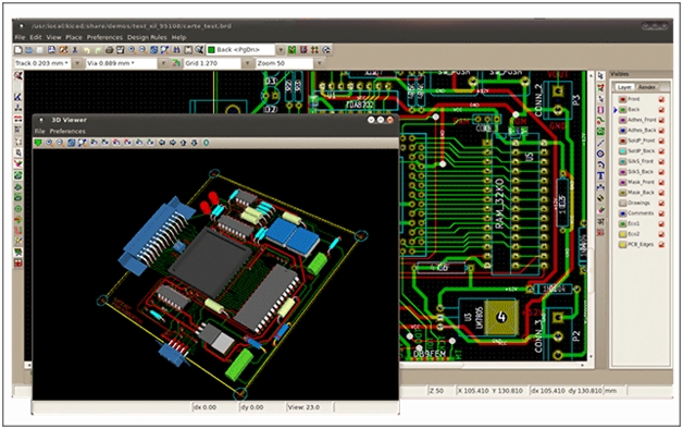
There is a need for specially designed tools and fixtures to enable adequate and accurate printing of the new IoT PCB’s. Let’s take for example, you are working with a rigid-flex kind of PCB which signifies that you will need a unique kind of tool peculiar to ensure that the board is totally kept flat. This therefore will ensure the proper and adequate printing of new IoT PCB’s with various thicknesses of the rigid and flex circuit portions
As we speak currently, we have several ventures and fresh developers now forming collaborations with EMS organizations who are specialized in PCB developments as a result of the pressing need to develop an efficacious and well-timed launch of new IoT PCB’s.
3. The Link Between IoT and Impending PCB Development.
The internet of things has provided a countless number of possible opportunities and discoveries as regard the PCB establishments. Though there is a lot of progress being made by circuit board developers with this particular technology. And beyond this, there is a lot more discoveries to come. Below we are going to take a look at the various incredible means by which IoT has impacted both the present and most importantly the future of PCB development.
a. It Goes Beyond Just Ordinary Designs
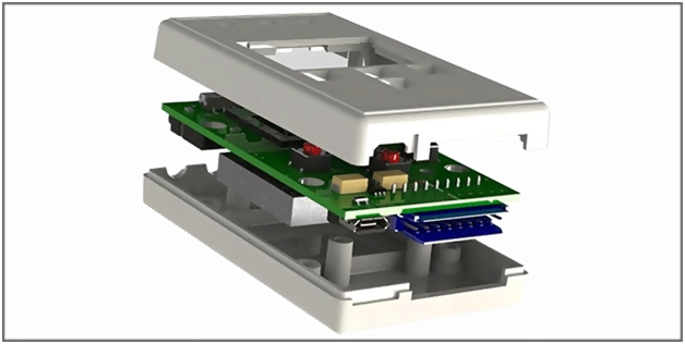
The process of PCB development entails a bit of labor division whereby the developers design a board and then give it to the mechanical group to carry out a thorough survey on the board to check if it’s a perfect fit. Afterwards it is handed over to the packaging group for the last fitting.
As a result of the little structural elements as well as progressively delicate parts, it is very important for each partner to be in agreement from the earliest starting point of the designing. So therefore, in order to blend capacity with structure as well as business needs impeccably, the formulation of new PCBs and computation of fitting must be done at the same time.
As internet of things keeps increasing in fame and popularity, PCB developers should anticipate to carry out more extensively virtual prototyping to be able to assess accurate some factors such as size of the board, total product weight, fitting of the board with the required and necessary enclosure, before handling the subtleties of the hardware.
Due to this, developers of PCB will at the time no more be considered as an impermanent entity as regards the development of PCB but will be referred to as professionals who laid emphasis on all the facets of design procedure.
- Institutionalization
In spite of the fact that right from the onset, there have been some principles guiding the development of PCBs, IoT is carrying the business towards a much increasingly homogenous future. PCBs made for IoT devices should maintain the largest amounts of productivity and unwavering quality.
As opposed to concentrating on remaking their circuitry to accomplish extraordinary outcomes, developers will probably decide to reuse obstructs that have just been reenacted and demonstrated to be fruitful in the field.
Sparing and reusing will turn into the standard in board advancement, and module configuration will entirely supplant customary schematic procedures.
- Partnership with a group of mechanical developers
When developing PCBs for IoT devices, there is need for a rigid connection as well as stronger collaboration between both the circuit board and mechanical developers.
Development procedures of items in the future will probably discard archaic and outdated assembly line models for a methodology where both mechanical and circuit changes and adjustments occur continuously.
Developers will never again need to change over documents starting with one programming design then onto the next to share board layouts and part models for fundamental impedance checks.
Rather, mechanical and electronic specialists will grasp the utilization of ECAD and MCAD instruments that unite their information for consistent, ongoing cooperation.
Obviously, this looming projection raises critical worries for most players in the ECAD business, whose plan utilities don’t function admirably together, let alone with MCAD programming.
The best apparatuses that would be ever developed will be those that get both the mechanical developers and circuit board designers in agreement.
- Reduction in Size
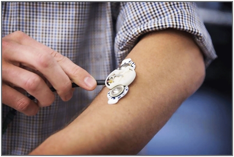
The era of developing well equipped IoT devices met its end giving designers adequate room to subside vias, tracks along with components. There was now a need for designers to create pocket sized gadgets that will function better and efficiently .

Let us take a look as the recent myriad of smartwatches in the market today. Although they are not as big as the normal watches, they still have better functions. An example is the Apple Watch pack which possesses sensors, an internal memory, LED displays, Bluetooth and so on.
Clients now want gadgets that are small and portable but still capable of performing day-to-day functions. With the look of things, due to the advent of rigid flex and HDI PCBs, normal traditional circuit boards will soon be outdated and considered unacceptable.
- Improved Packaging Technologies
Two common ways of packing gadgets over the years (through-hole and surface-mount packing) are now being replaced by recent technologies as gadgets progressively reduce in size.
Examples of these new technologies include Multi-Chip Modules and the System-in-Package Model. The Multi-Chip Module (MCM) assists PCB developers to link numerous ICs on a single die, making sure the form components are kept as thin as required. The System-in-Package on the other hand, incorporates three systems- the digital analogue and RF systems into one chip, whereas the ICs with three dimensions will enable piling of numerous silicon dies altogether to achieve a product with small size and lesser power consumption.
The utilization of these aforementioned new packing technologies stands to improve the printed boards, thereby paving way for a new era of PCBs that will provide designers with a greater rate per surface area ratio.
- Availability of new materials
In the recent world of Internet of Things, hardware is now designed to be smaller in size, less rigid and much more portable. Due to the utilization of a specialized kind of material known as FR4 necessary for developing square-shaped PCBs, is slowly creating a pathway for newly discovered materials such as plastic, flex-rigid copper or mesh.
In order to achieve a much greater success, FR4 developers have to form a collaboration with experts who are good with many materials.
Recently, the top two research establishments capable of providing consulting and testing services for wireless autonomous sensors and flexible circuitry are the Holst Centre and Wearable Technologies.
- Focus More On Wireless Connection
Modern PCB development are now laying more emphasis on wireless connectivity. This makes newly produced IoT PCBs to be able to interact with their environment, receive data and transfer them to both offline and online servers. Nowadays, designers have been filling up the market with wireless modules and RF circuits, thereby leaving behind their small impact without neglecting its effectiveness and efficiency. Nowadays, designers have been filling up the market with wireless modules and RF circuits, thereby leaving behind their small impact without neglecting its effectiveness and efficiency.
Those guidelines and principles which controls some factors would probably be renewed or updated in order to take care of the uprising needs. Factors such as security, data transfer speed and range. Another more interesting fact is that as institutionalization is gradually breaking grounds and taking over the place, it is not impossible to have only wireless technology governing over the entire future of the IoT realm.
- A More Intense Emphasis On the Consumption of Power
Most newly developed IoT products will most probably forfeit their mechanical power ports and plug-in sources in order to foster and encourage mobility as well as artificial brilliance. There is now a greater demand as the IoT marketplace is now advocating for more smart gadgets which can progressively with less intervention by human. However, PCB developers are required to focus more on the power consumption in order to pave wave for success in the nearest future.
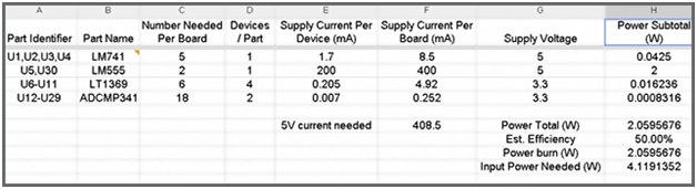
Developing a power budget for each functional component is a much encouraging option towards achieving an improved energy efficiency on PCBs rather than taking the whole product into consideration. This would improve the chances of developers to easily recognize and make the necessary changes to the components that require power.
- Human Body and PCBs
As the day goes by gradually, IoT designers are discovering new means by which life can be made much better than it is currently by exploring new options. There are some factors that should be taken into consideration as regards the nature of the human body when developing IoT products.
This has, however, posed a serious problem to PCB developers. An example of those factors is that the human possesses a lossy nature such that any gadget with the intention of being worn will require a very high signal strength in order to surmount the noise.
Also, there is a need to know that moisture and hardware do not go hand-in-hand, so therefore when developing IoT wearables, it is very crucial for the designers take note of the water and sweat effects.
New strategies have been put in place as mechanical developers have found a new way to design IoT products with the capacity to withstand moisture. Nevertheless, as new usefulness of IoT gadgets keep emerging, PCB developers will have to go an extra mile in order to make sure that some fragile portions are handled carefully
- Reliability
There is a need for high-level accuracy to be able to achieve small-sized devices. Even though majority of the developers out there prefer to interchange some parts on the normal circuit boards, still the IoT market cannot afford to fail due to some reasons.
There are some gadgets that must be functioning at all times. gadgets such as hearing aids and wristwatches. Due to the increasing demand on IoT gadgets, it is required for PCB developers to make sure that all boards are in perfect working conditions. This implies that they have to take their time to carefully carry out thorough optimization on the prototypes developed in order to ensure the best before moving on to the formulation of the product.
Conclusion
The aspect of electronic design is currently experiencing broad alterations to stay aware of IoT. Newly discovered methodologies are becoming the overwhelming focus and PCB developers are slowly holding onto the improvement of products all in all and not simply or merely the circuit board design.
As the interest for incredible circuit boards with small, light-weight portions extends much further, it is important to know that developers and formulators with the creative mind and the ability to exploit the new opportunities will profit significantly.
- What new PCB innovations are emerging due to IoT?
New designs involve rigid flex or flex circuit assemblies which differ from traditional bigger and flatter boards. - How do HDI methods benefit IoT device development?
HDI methods consume less power, perform better, and save space by increasing routing density while declining board surface area. - Why is collaboration between mechanical and circuit developers necessary?
Developers must collaborate to blend capacity with structure and business needs, often using ECAD and MCAD instruments for continuous adjustments. - What packing technologies are replacing through-hole and surface-mount methods?
Multi-Chip Modules and the System-in-Package Model are replacing older methods to keep form components thin and reduce size. - How does the human body affect IoT wearable PCB design?
The human body has a lossy nature requiring high signal strength, and moisture resistance is crucial because water and hardware do not go hand-in-hand. - What is the best way to manage power consumption in IoT products?
Developing a power budget for each functional component is an encouraging option to improve energy efficiency rather than considering the whole product. - Does the era of large circuit boards end with IoT?
Yes, the trend is toward pocket-sized gadgets, making normal traditional circuit boards soon outdated compared to rigid flex and HDI PCBs. - What materials are being explored alongside FR4 for IoT devices?
Specialized materials such as plastic, flex-rigid copper, or mesh are creating pathways for smaller and less rigid hardware.