Disassembling Apple’s diminutive inch-cube iPhone charger reveals a technologically advanced flyback switching power supply that goes beyond the typical charger. It simply takes AC input (anything between 100 and 240 volts) and produce 5 watts of smooth 5 volt power, but the circuit to do this is surprisingly complex and innovative.
How it works
The iPhone power adapter is a switching power supply, where the input power is switched on and off about 70,000 times a second in order to get the exact output voltage required. Because of their design, switching power supplies are generally compact and efficient and generate little waste heat compared to simpler linear power supplies.
In more detail, the AC line power is first converted to high voltage DC[1] by a diode bridge. The DC is switched on and off by a transistor controlled by a power supply controller IC. The chopped DC is fed into a flyback[2] transformer which converts it into low voltage AC. Finally, this AC is converted into DC which is filtered to obtain smooth power free of interference, and this power is output through the USB jack. A feedback circuit measures the output voltage and sends a signal to the controller IC, which adjusts the switching frequency to obtain the desired voltage.
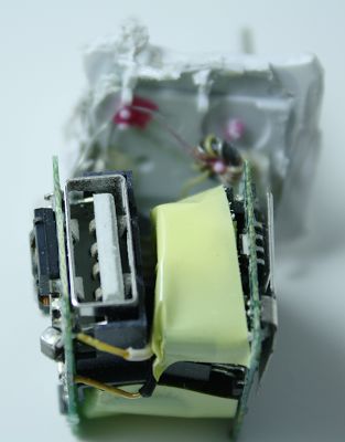
The side view above shows some of the larger components. The charger consists of two circuit boards, slightly under one inch square each.[3] The top board is the primary, which has the high voltage circuitry, and the bottom board, the secondary, has the low voltage output circuitry. The input AC first passes through a fusible resistor (striped), which will break the circuit if there is a catastrophic overload. The input AC is converted to high-voltage DC, which is smoothed by the two large electrolytic capacitors (black with white text and stripe) and the inductor (green).
Next, the high voltage DC is chopped at high frequency by a MOSFET switching transistor, which is the large three-pinned component in the upper left. (The second transistor clamps voltage spikes, as will be explained below.) The chopped DC goes to the flyback transformer (yellow, barely visible behind the transistors), which has low voltage output wires going to the secondary board below. (These wires were cut during disassembly.) The secondary board converts the low voltage from the transformer to DC, filters it, and then feeds it out through the USB connector (the silver rectangle in the lower left). The gray ribbon cable (just barely visible on the lower right under the capacitor) provides feedback from the secondary board to the controller IC to keep the voltage regulated.
The picture above shows the flyback transformer (yellow) more clearly, above the USB jack. The large blue component is a special “Y” capacitor[4] to reduce interference. The controller IC is visible above the transformer on the top of the primary board.[5]
The circuit in detail
The primary
The primary circuit board is packed with surface mounted components on both sides. The inner side (diagram above) holds the large components while the outer side (diagram below) has the controller IC. (The large components were removed in the diagrams, and are indicated in italics.) Input power is connected to the corners of the board, goes through the 10Ω fusible resistor, and is rectified to DC by the four diodes. Two R-C snubber circuits absorb EMI interference created by the bridge.[6] The DC is filtered by the two large electrolytic capacitors and the inductor, producing 125-340V DC. Note the thickness of the circuit board traces connecting these capacitors and other high-current components compared to the thin control traces.
The power supply is controlled by an 8-pin STMicrosystems L6565 quasi-resonant SMPS controller chip.[7] The controller IC drives the MOSFET switching transistor which chops the high voltage DC and feeds it into the primary winding of the flyback transformer. The controller IC takes a variety of inputs (secondary voltage feedback, input DC voltage, transformer primary current, and transformer demagnetization sensing) and adjusts the switching frequency and timing to control the output voltage through complex internal circuitry. The current sense resistors let the IC know how much current is flowing through the primary, which controls when the transistor should be turned off.
The second switching transistor, along with some capacitors and diodes, is part of a resonant clamp circuit that absorbs voltage spikes on the transformer. This unusual and innovative circuit is patented by Flextronics.[8][9]
The controller IC needs DC power to run; this is provided by an auxiliary power circuit consisting of a separate auxiliary winding on the transformer, a diode, and filter capacitors. Since the controller IC needs to be powered up before the transformer can start generating power, you might wonder how this chicken-and-egg problem gets solved. The solution is the high-voltage DC is dropped to a low level through startup power resistors to provide the initial power to the IC until the transformer starts up. The auxiliary winding is also used by the IC to sense transformer demagnitization, which indicates when to turn on the switching transistor.[7]
The secondary
On the secondary board, the low voltage AC from the transformer is rectified by the high-speed Schottky diode, filtered by the inductor and capacitors, and connected to the USB output. The tantalum filter capacitors provide high capacitance in a small package.
The USB output also has specific resistances connected to the data pins to indicate to the iPhone how much current the charger can supply, through a proprietary Apple protocol.[10] An iPhone displays the message “Charging is not supported with this accessory” if the charger has the wrong resistances here.
The secondary board contains a standard switching power supply feedback circuit that monitors the output voltage with a TL431 regulator and provides feedback to the controller IC through the optocoupler. A second feedback circuit shuts down the charger for protection if the charger overheats or the output voltage is too high.[11] A ribbon cable provides this feedback to the primary board.
Isolation
Because the power supply can have up to 340V DC internally, safety is an important issue. Strict regulations govern the separation between the dangerous line voltage and the safe output voltage, which are isolated by a combination of distance (called creepage and clearance), and insulation. The standards[12] are somewhat incomprehensible, but roughly 4mm of distance is required between the two circuits. (As I discuss in Tiny, cheap, dangerous: Inside a (fake) iPhone charger, cheap chargers totally ignore these safety rules.)
You might expect the primary board to have the dangerous voltages and the secondary board to have the safe voltages, but the secondary board consists of two areas: the hazardous area connected to the primary board, and the low-voltage area. The isolation boundary between these areas is about 6mm in the Apple charger and can be seen in the above diagram. This isolation boundary ensures that dangerous voltages cannot reach the output.
There are three types of components that cross the isolation boundary, and they must be specially designed for safety. The key component is the transformer, which provides a way for electrical power to reach the output without a direct electrical connection. Internally, the transformer is extensively insulated, as will be shown below. The second component type is the optocouplers, which send the feedback signal from the secondary to the primary. Internally, the optocoupler contains a LED and a photo-transistor, so the two sides are connected only by light, not by an electrical circuit. (Note the silicone insulation on the secondary side of the optocouplers to provide extra safety.) Finally, the Y capacitor is a special type of capacitor[4] that lets EMI (electromagnetic interference) escape between the high-voltage primary and the low-voltage secondary.
For more detail: Apple iPhone charger teardown