By Stephen Evanczuk
Contributed By Hearst Electronic Products
2014-12-17
For rapidly growing markets such as wearables or the Internet of Things (IoT), energy harvesting can significantly enhance battery life—or even enable battery-free designs. At the same time, however, engineers designing wearables and IoT devices face significant constraints in total design size and footprint. To meet growing demands for miniaturized systems, designers can turn to an array of highly integrated energy-harvesting ICs and wireless MCUs from silicon vendors including Atmel, CSR, Freescale Semiconductor, Linear Technology, Maxim Integrated, NXP Semiconductor, Silicon Laboratories, STMicroelectronics, and Texas Instruments, among others.
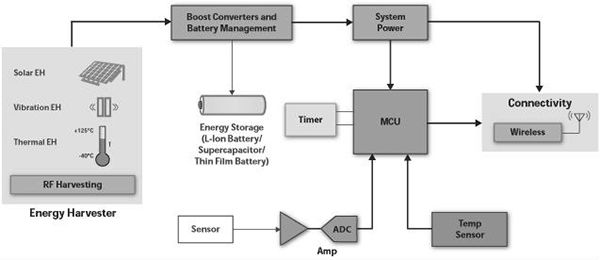
Energy harvesting offers tremendous benefits for applications able to take advantage of ambient-energy sources. Designers have employed energy-harvesting techniques to power applications ranging from motor and engine monitors to railway trackside electronics. Typically, these applications are based on wireless-sensor designs built to transmit sampled data about the environment or events of interest to a controller, aggregator, or other host (Figure 1).
Unlike other energy-harvesting applications, however, wearables and IoT devices share a need for designs that pack substantial functionality into the smallest possible package. Today, designers can take advantage of multiple options for reducing the footprint and overall size of these designs. For example, for a simple IoT localization application, a dynamic NFC/RFID tag, such as the STMicroelectronics M24LR16E could provide much of the required functionality in a package only 4.9 x 6.0 mm in size.
As with typical RFID tags, the M24LR16E powers itself by harvesting RF energy received from the RF reader, or vicinity coupling device (VCD). Unlike most RFID tags, however, the M24LR16E also features an energy-harvesting analog output that can be used to power additional devices such as an MCU. When placed in energy-harvesting mode, the M24LR16E-R outputs the excess energy coming from the RF field out to the Vout analog pin. Furthermore, designers can use the device’s ability to modulate the load on the received carrier to communicate with the VCD at rates up to 53 Kbps—eliminating the need for a separate wireless RF transceiver.
For more detail: MOSFET Gate Drivers from Diodes Incorporated Boosts Conversion Efficiency

